
Shunlongwei Co. ltd.
IGBT Module / LCD Display Distributor
Customer Service
+86-755-8273 2562
IGBT Module / LCD Display Distributor
“At the SFF Foundry Forum in the United States last week, Samsung released a new generation of logic process roadmap. 3nm process will be mass-produced in 2021, and the new generation GAA transistor process will be used for the first time, which is one year ahead of its rival TSMC. Leading Intel Corporation for at least 2-3 years.
“
At the SFF Foundry Forum in the United States last week, Samsung released a new generation of logic process roadmap. 3nm process will be mass-produced in 2021, and the new generation GAA transistor process will be used for the first time, which is one year ahead of its rival TSMC. Leading Intel Corporation for at least 2-3 years.
In addition to the 3nm process, Samsung has actually prepared a variety of other processes, covering every number from the 14, 10nm node down, and in the future, it will enter the 2nm or even 1nm process below 3nm, which will challenge the physics of semiconductors. Learn the limit.
This also brings up another problem, that is, everyone feels very confused about Samsung’s process technology. For example, Qualcomm’s Snapdragon processor has 10nm process, 11nm process, and 8nm process. There may be 6nm and 5nm processes in the future. What are the differences between these processes?
Cacdence’s official blog columnist Paul McClellan wrote an article a few days ago to analyze Samsung’s process technology, using a concise and clear icon to summarize Samsung’s current process technology, as shown below:
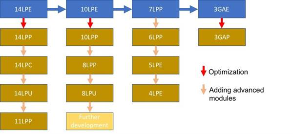
Samsung’s current process is actually divided into four major nodes, namely 14nm, 10nm, 7nm and 3nm. There will be multiple derivative versions for each generation node. Among them, the 14nm node has 14nm LPE, 14nm LPP, 14nm LPC, 14nm LPU and 11nm. LPP version, 10nm node has 10nm LPE, 10nm LPP, 8nm LPP, 8nm LPU and the version still under development.
In the 7nm node, Samsung gave up the low power consumption of LPE this time, and directly entered 7nm LPP (and EUV lithography process assistance), 6nm LPP, 5nm LPE, 4nm LPE and other derivative versions.
The real major change is the 3nm node, because 3nm will abandon FinFET and switch to GAA transistors. The first generation is the 3GAE process, and there is an optimized version of the 3GAP process, which is still being optimized and improved in the future.
The timing of each process of Samsung is also different. The 7nm EUV process will start mass production in April this year, and the 6nm process will be introduced in the second half of this year. The 5nm process will be developed in April this year.
The development of the 4nm process is completed in the second half of this year, and the 3nm GAE process has released version 1.0 of the PDK, which is expected to be mass-produced in 2021.
The Links: M150XN05-V6 DSEI2X61-12A
