
Shunlongwei Co. ltd.
IGBT Module / LCD Display Distributor
Customer Service
+86-755-8273 2562
IGBT Module / LCD Display Distributor
“It’s normal, almost reasonable, for an app to be developed that doesn’t seem to have a solution. To meet application requirements, we needed to come up with a solution that exceeded the performance of existing products on the market. For example, an application may require an amplifier with high speed, high voltage, high output drive capability, and may also require excellent DC accuracy, low noise, low distortion, etc.
“
Author: Jino Loquinario Analog Devices
Introduction
It’s normal, almost reasonable, for an app to be developed that doesn’t seem to have a solution. To meet application requirements, we needed to come up with a solution that exceeded the performance of existing products on the market. For example, an application may require an amplifier with high speed, high voltage, high output drive capability, and may also require excellent DC accuracy, low noise, low distortion, etc.
Amplifiers that meet speed and output voltage/current requirements as well as amplifiers with excellent DC accuracy are readily available in the market, and indeed many are. However, all of these requirements may not be met by a single amplifier. When faced with such a problem, some people think that we cannot meet the requirements of this type of application, we must settle for a mediocre solution, either with a precision amplifier or with a high-speed amplifier, possibly sacrificing some requirements. Fortunately, this is not entirely true. One solution to this is to use a composite amplifier, and this article will show how this is accomplished.
composite amplifier
A composite amplifier consists of two separate amplifiers configured in such a way that one can realize the advantages of each amplifier while attenuating the disadvantages of each amplifier.
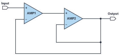
Figure 1. Simple Composite Amplifier Configuration
Referring to Figure 1, the AMP1 has the excellent DC accuracy and noise and distortion performance required by the application. AMP2 meets the output drive requirements. In this configuration, the amplifier with the desired output specification (AMP2) is placed in the feedback loop of the amplifier with the desired input specification (AMP1). Some of the techniques involved in this configuration and its benefits are discussed below.
set gain
When first encountering a composite amplifier, the first question may be how to set the gain. To solve this problem, it is helpful to think of the composite amplifier as a single non-inverting op amp contained within a large triangle, as shown in Figure 2. Imagine the big triangle is black and we can’t see what’s inside, then the gain of the non-inverting op amp is 1 + R1/R2. Uncovering the composite configuration inside the big triangle didn’t change anything, the gain of the whole circuit is still controlled by the ratio of R1 and R2.
In this configuration, it would be tempting to think that changing the gain of AMP2 through R3 and R4 would affect the output level of AMP2, indicating that the composite gain would change, but this is not the case. Increasing the gain around AMP2 via R3 and R4 only reduces the effective gain and output level of AMP1, while the composite output (AMP2 output) remains the same. Alternatively, reducing the gain around AMP2 will increase the effective gain of AMP1. Therefore, the gain of the composite amplifier generally depends only on R1 and R2.
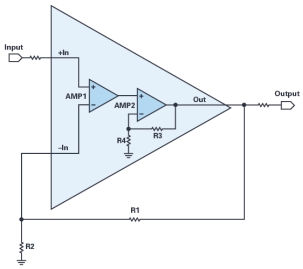
Figure 2. Composite amplifier treated as a single amplifier
This article will discuss the main advantages and design considerations for implementing a composite amplifier configuration. This article will focus on its impact on bandwidth, DC accuracy, noise and distortion.
Bandwidth expansion
One of the main advantages of implementing a composite amplifier is wider bandwidth compared to a single amplifier configured for the same gain.
Referring to Figures 3 and 4, assume we have two independent amplifiers, each with a gain-bandwidth product (GBWP) of 100 MHz. Combine them into a composite configuration and the effective GBWP of the entire combination will increase. At unity gain, the -3 dB bandwidth of the composite amplifier is about 27% higher, albeit with a small amount of peaking. This advantage becomes more pronounced at higher gains.
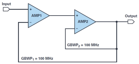
Figure 3. Unity-Gain Composite Amplifier
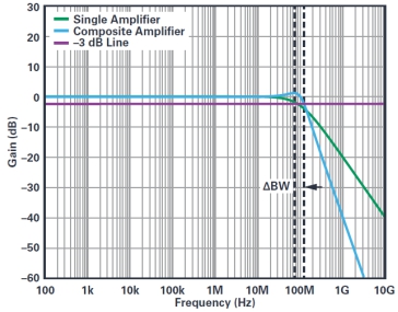
Figure 4. -3 dB Bandwidth Improvement at Unity Gain
Figure 5 shows a composite amplifier with a gain of 10. Note that the composite gain is set to 10 by R1 and R2. The gain around AMP2 is set to about 3.16, forcing the effective gain of AMP1 to be the same. Dividing the gain equally between the two amplifiers yields the largest possible bandwidth.
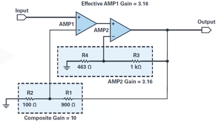
Figure 5. Composite Amplifier Configured for Gain of 10
Figure 6 compares the frequency response of a single amplifier with a gain of 10 to that of a composite amplifier configured for the same gain. In this case, the -3 dB bandwidth of the composite amplifier is about 300% higher. How is this possible?
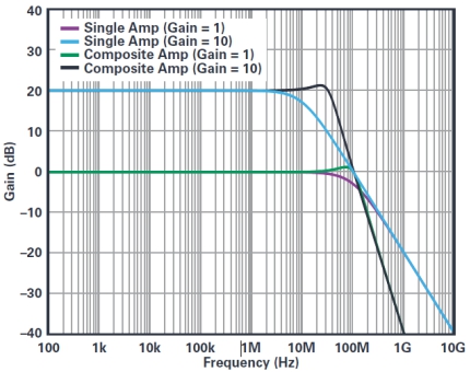
Figure 6. -3 dB bandwidth improvement at a gain of 10
See Figure 7 and Figure 8 for specific examples. We require a system gain of 40 dB, using two identical amplifiers, each with an open loop gain of 80 dB, and a GBWP of 100 MHz.
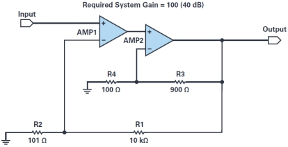
Figure 7. Distributing gain for maximum bandwidth
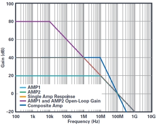
Figure 8. Expected Response of a Single Amplifier
To achieve the highest possible bandwidth for the combination, we will divide the desired system gain equally between the two amplifiers, each with a gain of 20 dB. Therefore, setting the closed-loop gain of AMP2 to 20 dB will force the effective closed-loop gain of AMP1 to be 20 dB as well. With this gain configuration, the operating points of both amplifiers on the open-loop curve are lower than either amplifier’s operating point at 40 dB gain. Therefore, the composite amplifier will have a higher bandwidth at a gain of 40 dB than a single amplifier solution of the same gain.
While seemingly relatively simple and easy to implement, appropriate measures should be taken when designing a composite amplifier to obtain the highest possible bandwidth without sacrificing the stability of the combination. In practical applications, amplifiers have non-ideal characteristics and may not be identical, which requires proper gain configuration to maintain stability. Also note that the composite gain will roll off at -40 dB/decade, so care must be taken when distributing the gain between the two stages.
In some cases, evenly distributing the gain may not be possible. In this regard, to distribute the gain equally between the two amplifiers, the GBWP of AMP2 must always be greater than or equal to the GBWP of AMP1, otherwise peaking will result and possibly circuit instability. In situations where the AMP1 GBWP must be greater than the AMP2 GBWP, redistributing the gain between the two amplifiers can often correct the instability. In this case, reducing the gain of AMP2 results in an increase in the effective gain of AMP1. The result is that the AMP1 closed-loop bandwidth is reduced because its operating point on the open-loop curve is increased, and the AMP2 closed-loop bandwidth is increased because its operating point is decreased on the open-loop curve. If the deceleration of AMP1 and the acceleration of AMP2 are fully applied, the stability of the composite amplifier is restored.
This article selects AD8397 as the output stage (AMP2), which is connected with the amplifier AMP1 of various precisions to demonstrate the advantages of the composite amplifier. The AD8397 is a high output current amplifier capable of delivering 310 mA.
Bandwidth extension in combination with amplifier, gain of 10, VOUT = 10 Vpp
|
amplifier |
Single Amplifier Bandwidth (kHz) |
Composite Amplifier Bandwidth (kHz) |
Bandwidth Expansion % |
|
ADA4091 |
30 |
94 |
213 |
|
AD8676 |
165 |
517 |
213 |
|
AD8599 |
628 |
2674 |
325 |
Maintain DC accuracy
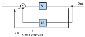
Figure 9. Op amp feedback loop
In a typical op amp circuit, a portion of the output is fed back to the inverting input. The error present at the output (generated in the loop) is multiplied by the feedback factor (β) and then subtracted. This helps maintain the fidelity of the output with respect to the input multiplied by the closed-loop gain (A).
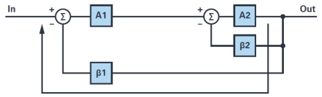
Figure 10. Composite Amplifier Feedback Loop
For a composite amplifier, amplifier A2 has its own feedback loop, but both A2 and its feedback loop are within the larger feedback loop of A1. The output now contains the larger errors caused by A2, which are fed back to A1 and corrected. A larger correction signal results in the accuracy of A1 being preserved.
The effect of this composite feedback loop can be clearly seen in the circuit shown in Figure 11 and the results shown in Figure 12. Figure 11 shows a composite amplifier consisting of two ideal op amps. The composite gain is 100 and the AMP2 gain is set to 5. VOS1 represents the 50µV offset voltage of AMP1, while VOS2 represents the variable offset voltage of AMP2. Figure 12 shows that when VOS2 When sweeping from 0 mV to 100 mV, the output offset is not affected by the magnitude of the error (offset) contributed by AMP2. Instead, the output offset is only proportional to the error in AMP1 (50µV times the composite gain of 100), and regardless of VOSWhat is the value of 2, it all stays at 5 mV. Without the composite loop, we would expect the output error to be as high as 500 mV.
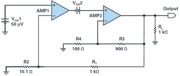
Figure 11. Offset Error Contribution
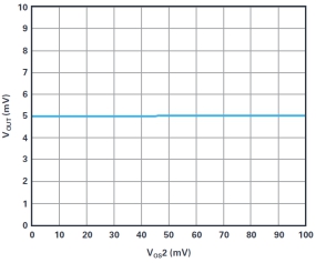
Figure 12. Composite Output Offset vs. VOS2 relationship
Table 2. Output Offset Voltage at Gain of 100
|
amplifier |
Effective VOS (mV) |
VOSDrop (composite configuration) |
|
AD8397 |
100 |
|
|
AD8397 + ADA4091 |
3.5 |
28.6× |
|
AD8397 + AD8676 |
1.2 |
83.3× |
|
AD8397 + AD8599 |
1 |
100× |
noise and distortion
The output noise and harmonic distortion of the composite amplifier are corrected in a similar manner to the DC error, but for the AC parameters, the bandwidth of the two stages also plays a role. We will use an example to illustrate this using output noise; with the understanding that distortion cancellation works in much the same way.
Referring to the circuit shown in Figure 13, as long as the first stage (AMP1) has sufficient bandwidth, it will correct the larger noise of the second stage (AMP2). When the bandwidth of AMP1 starts to run out, the noise from AMP2 will start to dominate. However, if the AMP1 has too much bandwidth and there is peaking in the frequency response, then there will be noise peaks at the same frequency.
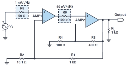
Figure 13. Noise Sources for Composite Amplifiers
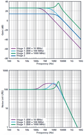
Figure 14. Noise Performance vs Bandwidth of the First Stage
For this example, resistors R5 and R6 in Figure 13 represent the inherent noise sources for AMP1 and AMP2, respectively. The upper curve of Figure 14 shows the frequency response of various AMP1 bandwidths and the frequency response of AMP2 for a single fixed bandwidth. Recall from the Gain Distribution section, if the composite gain is 100 (40 dB) and the AMP2 gain is 5 (14 dB), the effective gain for AMP1 will be 20 (26 dB), as shown here.
The lower curve shows the broadband output noise density for each case. At low frequencies, the output noise density is dominated by AMP1 (1 nV/√HZ times 100 composite gain equals 100 nV/√HZ). This will continue as long as AMP1 has enough bandwidth to compensate for AMP2.
If the AMP1 bandwidth is less than the AMP2 bandwidth, when the AMP1 bandwidth begins to roll off, the noise density will start to be dominated by AMP2. This can be seen in the two traces in Figure 14, where the noise rises to 200 nV/√HZ (40 nV/√HZ times the gain of 5 for AMP2). Finally, if AMP1 has a much larger bandwidth than AMP2, causing the frequency response to peak, the composite amplifier will exhibit noise peaks at the same frequency, as shown in Figure 14. The magnitude of the noise peaks will also be higher due to excessive gain caused by frequency response peaking.
Tables 3 and 4 show the effective noise reduction and THD+n improvement, respectively, when using different precision amplifiers as the first stage to form a composite amplifier with the AD8397.
Table 3. Noise reduction using different front-end amplifiers, effective gain = 100, f = 1 kHz
|
configure |
Noise, en (nV/√HZ) |
Effective noise reduction (%) |
|
AD8397 only |
450 |
|
|
AD8397 + ADA4084 |
390 |
13.33 |
|
AD8397 + AD8676 |
280 |
37.78 |
|
AD8397 + AD8599 |
107 |
76.22 |
Table 4. Comparison of THD+n using different front-end amplifiers, effective gain = 10, f = 1 kHz, ILOAD = 200 mA
|
configure |
Effective THD+n (dB) |
THD+n improvement (dB) |
|
AD8397 only |
C100.22 |
|
|
AD8397 + ADA4084 |
C105.32 |
5.10 |
|
AD8397 + AD8676 |
C106.68 |
6.46 |
|
AD8397 + AD8599 |
C106.21 |
5.99 |
system level application
In this example, the DAC output buffer application is targeting a 10 V pp output for a low impedance probe at 500 mA pp, requiring low noise, low distortion, excellent DC accuracy, and the highest possible bandwidth. The 4 mA to 20 mA current output by the DAC will be converted to a voltage by the TIA and then converted to the input of the composite amplifier for further amplification. The AD8397 at the output can meet the output requirements. The AD8397 is a rail-to-rail, high output current amplifier capable of delivering the required output current.
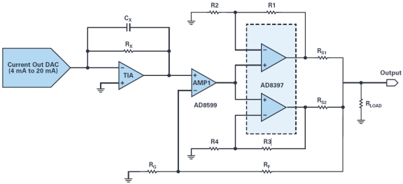
Figure 15. Application circuit for DAC output driver
AMP1 can be any precision amplifier with the DC accuracy required for the configuration. In this application, various front-end precision amplifiers can be used with the AD8397 (and other high output current amplifiers) to achieve the excellent DC accuracy and high output drive capability required by the application.
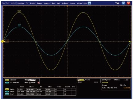
Figure 16. V of AD8599 and AD8397 Composite AmplifiersOUTand IOUT
Table 5. AD8599+AD8397 Composite Amplifier Specifications
|
parameter |
value |
|
gain |
10V/V |
|
−3 dB bandwidth |
1.27MHz |
|
The output voltage |
10 Vpp |
|
Output current |
500 mA pp |
|
Output offset voltage |
102.5 μV |
|
Voltage Noise (f = 1 kHz) |
20.95nV/√Hz |
|
THD+n (f = 1 kHz) |
C106.14dB |
This configuration is not limited to the AD8397 and AD8599, other amplifier combinations are possible as long as the output drive requirements are met and excellent dc accuracy is provided. The amplifiers in Table 6 and Table 7 are also suitable for this application.
Table 6. Amplifiers with High Output Current Drive Capability
|
High output current amplifier |
Current drive (A) |
Slew rate |
VSRange, Maximum (V) |
|
ADA4870 |
1 |
2.5kV/μs |
40 |
|
LT6301 |
1.2 |
600 V/μs |
27 |
|
LT1210 |
2 |
900 V/μs |
36 |
Table 7. Precision Front End Amplifier
|
Precision Amplifier |
VOS (μV) |
VNOISE, en (nV/√HZ) |
THD+n, 1 kHz (dB) |
|
LT6018 |
50 |
1.2 |
C115 |
|
ADA4625 |
80 |
3.3 |
C110 |
|
ADA4084 |
100 |
3.9 |
C90 |
in conclusion
The two amplifiers are combined into a composite amplifier that achieves the best specifications of each amplifier while compensating for the limitations of each. Amplifiers with high output drive capability combined with precision front-end amplifiers provide solutions for very difficult applications. It is important to consider stability, noise peaking, bandwidth, and slew rate when designing for optimum performance. There are many possible solutions to meet various application requirements. The right implementation and combination can achieve the right balance of applications.
Thanks
The authors are grateful to Zoltan Frasch and Bruce Petipas for their technical contributions to this article.
About the Author
Jino Loquinario joined Analog Devices in 2014 and is currently a product applications engineer in the Linear Products and Solutions Group. He graduated from the University of Science and Technology of the Philippines, Visayas, with a bachelor’s degree in electrical engineering. Contact information:[email protected]


