
Shunlongwei Co. ltd.
IGBT Module / LCD Display Distributor
Customer Service
+86-755-8273 2562
IGBT Module / LCD Display Distributor
Isolation drive is widely used in industrial products, and the design of its power supply isolated power supply is a key part of the isolation drive design. Traditional isolated drive power supply solutions mostly use flyback or push-pull structures. Compared with these two solutions, LLC resonant converters have their own unique advantages, such as high power density, low noise, and low cost.
Due to the reliability and redundancy of the system, the centralized control power supply architecture has gradually developed to a distributed open-loop method. Open-loop control, such as a push-pull structure with a 50% duty cycle, is widely used in scenarios that provide isolated power supply. However, the high dv/dt of the secondary side will be coupled to the primary side through the parasitic capacitance of the primary and secondary side of the transformer, causing noise and even affecting the operation of the primary side controller.
If you want to reduce the parasitic capacitance of the primary and secondary sides of the transformer, you can increase the distance between the primary and secondary sides of the transformer or use a transformer tank structure. However, this will increase the leakage inductance of the transformer. The increase in leakage inductance will produce voltage spikes that increase the stress of the switching tube, and the energy of the leakage inductance will cause greater power loss and affect the efficiency of the power supply. In order to use transformers with smaller parasitic capacitance and larger leakage inductance without reducing system performance, LLC resonant converters can be used. In this isolation topology, when the leakage inductance of the transformer is large, the resonant capacitor can compensate for it.
TI’s latest UCC25800-Q1 open-loop LLC transformer drive control chip integrates half-bridge power Circuits, control circuits, and protection circuits to simplify the design of isolated power supplies. The advantages of the LLC resonant converter described above over other isolated power solutions can be realized by this controller, which can minimize the EMI noise generated by the high-speed switching devices. And because of the unique soft switching characteristics of LLC topology, the noise of the whole converter will be reduced and the efficiency will be improved.
1 Brief introduction of UCC25800-Q1
UCC25800-Q1 is an open-loop LLC driver that integrates a half-bridge power Circuit (including MOS driver), control circuit, protection circuit, etc. In addition to the above-mentioned compensation for transformer leakage inductance and reduction of conducted noise on the primary and secondary sides of the transformer, the soft-start function in this control chip also significantly reduces the inrush current when the converter is turned on. In addition, the features of UCC25800-Q1 are as follows:
• 9~34V input voltage range
• Very low EMI
• Maximum output power of 6W at 24V input
• The switching frequency of 100kHz~1.2MHz can be set by external resistance, and it can also be synchronized by external
• The maximum dead time can be set
• Input over-voltage and under-voltage protection, output over-current protection (protection threshold can be adjusted), chip over-temperature protection
• The control IC can be switched off externally
• System intelligent fault code output function
• 8-pin DGN package
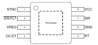
The pin function and brief introduction of UCC25800-Q1 are as follows:
|
Pin |
Pin function |
Remark |
|
SYNC |
External synchronization clock signal input |
When using this pin for synchronization, the drive signal of the half-bridge inverter MOS inside the controller is generated on the rising edge of the SYNC pin voltage, so the switching frequency is half of the synchronization signal frequency. When this function is not used, this pin can be connected to any resistance to the ground or directly open. |
|
|
Controller turn-off pin (turn off when low level) and fault code output pin |
The fault information of the converter can be viewed through this pin. |
|
VREG |
Reference voltage output pin (5V) |
The layout of the decoupling capacitor between the output of this pin and GND should make the entire loop as short as possible. |
|
OC/DT |
This pin is used to configure the maximum dead time and overcurrent protection threshold of the half-bridge circuit in the converter |
See the configuration method below. |
|
VCC |
The power supply pins of the converter and control chip. |
The layout of the filter capacitor between this pin and GND should make the loop as short as possible to improve efficiency and reduce EMI noise. |
|
SW |
Output pin of half bridge circuit |
|
|
GND |
GND pin of converter and controller |
|
|
RT |
Converter switching frequency configuration pin |
The specific configuration method of the converter switching frequency is shown below. |
2 Typical design reference based on UCC25800-Q1
In this part, in order to facilitate specific explanations, this section takes an isolated power supply design based on UCC25800-Q1 as an example to illustrate the selection of chip peripheral component parameters and system parameters in detail. The design parameters of this power supply are as follows:
• Switching frequency 1MHz;
• Input voltage +15V, single-channel input, three-channel isolated output;
• Output voltage +15V/-5V;
• Single output power 2W;
The secondary side of the circuit uses a voltage doubler rectification method, which is commonly used in high voltage and low current application scenarios. The topology of the entire circuit is shown in Figure 2, where Lm is the magnetizing inductance of the transformer, and Lr is the equivalent leakage inductance of the transformer. The leakage inductance is resonated by the capacitor of the voltage doubler rectification. The output voltage amplitude of the half-bridge circuit is 0.5*VIN, and the voltage amplitude doubles after the voltage is doubled. When considering the conduction voltage drop (VF) of the rectifier diode, the DC gain of the entire converter can be calculated with the following formula:
![]()
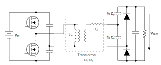
Figure 2 LLC resonant converter
2.1 Frequency setting (SYNC pin and RT pin)
According to the DC gain characteristics of the LLC resonant converter, it can be divided into three working areas, as shown in Figure 3. In this figure, the horizontal axis is the per-unit value of the switching frequency based on the resonance frequency, and the vertical axis is the voltage gain of the circuit.
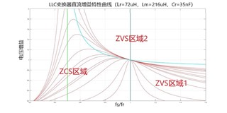
Fig. 3 DC characteristic curve of LLC
When the switching frequency fsw of the LLC resonant converter is set to different values, the working state of the converter is also different (fr in the figure is the resonant frequency of the series resonance of Cr and Lr in the converter, and frp is the common combination of Cr and Lr and Lm. Resonant frequency at series resonance):
When working in zone 1 and zone 2, the input impedance of the converter is inductive, and the MOSFET of the half-bridge circuit works in the ZVS (Zero Voltage Switching) zone. When the switching frequency of the converter is greater than fr, the diode on the secondary side works in current continuous mode, and ZCS (Zero Current Switching) cannot be realized, and reverse recovery loss will occur.
When working in zone 3, the input impedance of the converter is capacitive, and the MOSFET of the half-bridge circuit works in the ZCS zone. When the MOSFET implements ZCS, the loss will be larger than ZVS.
When using UCC25800-Q1 to design the converter, whether it is using an external synchronization signal or RT pin resistance to set the frequency inside the chip, the switching frequency should be designed to be 90% of the resonant frequency.
There are two situations for setting the switching frequency, there are two kinds of external synchronization signal (SYNC pin) and no external synchronization signal.
When there is no external synchronization signal, the switching frequency of the converter is set by the resistance of the RT pin. The switching frequency is fsw=RRT*10Hz/Ω. If the pin is open or the resistance exceeds 100kΩ, the system will work at the default 1.2MHz.
When there is an external synchronization signal, the external synchronization signal is ignored during the 1.5ms soft start process. After the soft start is over, if a certain frequency range (2.3 times to 2.6 times the frequency set by the RT pin resistance) is satisfied, the converter will use this signal to work. If the frequency of the synchronization signal is not within the range, use the switching frequency set by the RT pin to work.
If you want to make a fixed output LLC resonant converter, you can directly set a fixed switching frequency through the RT pin. Then select the resonant capacitor of the corresponding parameter according to the leakage inductance of the transformer. If you want to synchronize through the external input square wave synchronization signal of the SYNC pin, the frequency of the external input should be within the frequency range configured by the RT pin. If effective frequency and voltage regulation is required during design and debugging, a transformer with a smaller ratio of magnetizing inductance to leakage inductance Lp/Ls should be selected to narrow the frequency range for obtaining the same gain.
Design example:
The switching frequency of the designed isolated power supply is 1MHz, and the frequency of the converter can be configured through the RT pin. At this time, the SYNC pin can be opened. Theoretically, RRT should be 100kΩ, and in practical applications we use 97.6kΩ. The schematic diagram of the circuit is shown in Figure 5.
2.2 The maximum dead time of the converter, overcurrent protection point setting (OC/DT pin)
The maximum dead time setting of the converter:
A dead time should be set between the two switch tubes of the same bridge arm of the half-bridge circuit to avoid direct current flow through the circuit. At the same time, the parasitic capacitance between the drain and source of the switch tube in the LLC resonant converter is fully discharged during the dead time to achieve effective ZVS and reduce loss and EMI noise.
This pin sets the maximum dead time by setting the voltage at this point. Usually we can choose 5%~10% of the switching period as the maximum dead time.
The maximum dead time within a certain range can be configured according to the following formula:
DTMAX=150ns*V/(VOC/DT-0.9V) (2)
VOC/DT=150ns*V/DTMAX+0.9V (3)
The formula (3) configures the peripheral circuit according to the required dead time.
In other cases, the corresponding pin voltage and maximum dead time are as follows:
|
OC/DT pin voltage |
Maximum dead time |
|
|
Trigger short circuit protection, the device shuts down |
|
0.5VOC/DT |
1.25µs |
|
1V |
See manual curve |
|
3.9V |
50ns minimum |
|
3.95V |
Beyond the range, the device shuts down |
The overcurrent protection mechanism of the converter:
UCC25800-Q1 provides two protection mechanisms: OCP1 only samples the lower tube of the half-bridge circuit. If the lower tube current exceeds the overcurrent protection point (IOCP) in each switching cycle within 2ms, OCP1 protection will be triggered; OCP2 samples both the upper and lower tubes, and when the upper and lower tube current exceeds 5 times the IOCP overcurrent protection point , When it is longer than 100ns, OCP2 protection is triggered.
In addition, during the soft start, OCP1 is disabled, and the threshold of OCP2 is fixed at 5*IOCPMAX (5A). After the soft start, OCP1 starts to be enabled, and the threshold is IOCP. The threshold of OCP2 becomes 5*IOCP. The IOCP here can be configured by the user. When OCP1 or OCP2 is triggered, the control chip’s turn-off time and other mechanisms are detailed in Figure 12-9 and Figure 12-10 in the manual.
Overcurrent protection point configuration of the converter:
There is a 50µA DC source inside the UCC25800-Q1 OC/DT pin. The DC source is used to set the size of the IOCP, which is done by configuring the Thevenin equivalent resistance outside the OC/DT pin. The specific configuration relationship is shown in the following table:
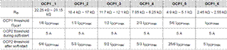
Set Rth according to Table 1 (this resistance is the parallel connection of the up/down voltage divider resistance of the pin, which is the Thevenin equivalent resistance mentioned above). According to the maximum dead time (pin multiplexing), the specific up/down voltage divider resistance value can be calculated.
Design example:
In this design, the converter switching cycle is 1000ns, and the maximum dead time is 5%~10% of the switching cycle, so the pin voltage should be about 3.9V. Secondly, if the three outputs are all 20V/1.2W, the output current is 3*1.2W/20V=180mA. To set the circuit’s overcurrent protection, you need to calculate the output current of the SW pin of UCC25800-Q1. The calculation process is as follows:
• The effective value of the secondary side current of the voltage doubler rectifier is Irms-s=π*IOC/1.414=399.92mA;
• The effective value of the primary current is Irms-p=Irms-s*1.5=599.88mA;
• The peak value of the primary current is IpKp=599.88mA*1.414=848.36mA;
Reserve a margin of 30%~50% of the primary current peak value, and the current protection threshold is 1102.4mA~1272mA, which exceeds 1A, so the OCP setting is OCP1_6, and Rth should be between 2.45kΩ and 2.55kΩ. Finally, after calculation, the upper divider resistance is 3.24 kΩ and the lower divider resistance is 12.4 kΩ. The schematic diagram is shown in Figure 5.
2.3 Main circuit design reference:
2.3.1 Selection of transformer
Determine the turns ratio according to the input and output voltage
Select the transformer according to the power level and the rated current of the primary and secondary side current
Select magnetic material according to frequency
Select the magnetic core according to the volt-microsecond product of the transformer
In the selection of the transformer, try to choose a trough transformer with a smaller coupling capacitance between the primary and secondary sides to minimize the conduction of noise. The selection of other circuit components will be described in the reference design together with the transformer.
Transformer selection reference:
In this example, the transformer turns ratio is 15V/(20V+1V), where 1V is about the voltage drop of two Schottky diodes, and the theoretical turns ratio is 1:1.4. The peak currents of the primary and secondary sides are 848mA and 565mA respectively. The volt-microsecond product of the primary side of the transformer is 1.875V·s. The final transformer selected is Wuerth Elektronik’s 760301107, with a turns ratio of 1:1.5 and a volt-microsecond product of 40.8V.・ S, see the manual for the specific parameters of the transformer.
2.3.2 Selection of resonant capacitor
The LLC resonant converter should work in an under-resonant state, so the resonant frequency can be set to 1.1~1.15 times the switching frequency, and then the value of Cr can be calculated based on the series resonance of Cr and Lr. Can refer to the following formula:
![]()
The switching frequency is 1MHz, and the resonance frequency should be between 1.1MHz and 1.15MHz. The leakage inductance of the transformer is 2.9uH, and finally calculated Cr should be 6.6nF~7.22nF. The two capacitors in the voltage doubler rectification are respectively 3.3nF~3.61nF, which are half of the resonant capacitor. The final selected capacitor is GRM216R71H332KA01D, 3.3nF.
2.3.3 Adding balance resistance
The two ends of the capacitor of the half-bridge inverter circuit should be connected in parallel with balancing resistors to make the voltage equalizing ability of the capacitor stronger when the converter is working, and to avoid the transient current impact triggering when the chip is powered by VCC and is turned off for a long time. Stream protection. In this example, a 100kΩ resistor is connected in parallel at both ends of the two capacitors connected in series.
2.3.4 Selection of rectifier diode
In addition to considering the withstand voltage level and current capacity of the rectifier diode, Schottky diodes should also be selected for the switching frequency. In this example, PMEG6010CEGWJ is selected.
2.3.5 Generation of negative pressure
In the design context, two outputs of 15V/-5V are required. There are several ways to divide the voltage into two for reference:
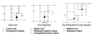
Figure 4 Separate single output into a two-way solution
In this example, the first method is used to separate the output, and a 5.1V voltage regulator tube is selected to generate negative pressure. If high voltage regulation accuracy is required, 2 or 3 methods can be used. Method 2 adds a voltage reference at the negative pressure terminal to achieve negative voltage stabilization. In mode 3, when a voltage reference is used at the negative voltage end, a linear voltage stabilizing circuit is added at the positive voltage end to realize the voltage stabilization of the positive end.
3 Reference design schematics and test results
3.1 Reference design schematic
The schematic diagram of the reference design is shown in Figure 5:
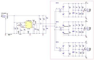
Figure 5 Schematic of the reference design
3.2 Design results and analysis
1) Output voltage adjustment rate and efficiency
|
Input voltage (V) |
Input current (mA) |
Output positive voltage |
Positive voltage output accuracy |
Positive voltage load current (mA) |
Output negative voltage |
Negative voltage output accuracy |
Negative voltage load current (mA) |
efficient |
|
15 |
286 |
14.56 |
-2.93% |
55.6 |
-5.1482 |
2.96% |
52.9 |
75.66% |
|
15 |
265 |
14.836 |
-1.09% |
50.2 |
-5.1514 |
3.03% |
48.2 |
74.95% |
|
15 |
244 |
15.097 |
0.65% |
45.4 |
-5.1577 |
3.15% |
43.3 |
74.49% |
|
15 |
220 |
15.396 |
2.64% |
38.8 |
-5.1577 |
3.15% |
38.2 |
72.22% |
|
15 |
198 |
15.682 |
4.55% |
34.2 |
-5.1556 |
3.11% |
33 |
71.36% |
|
15 |
158 |
16.242 |
8.28% |
25 |
-5.1647 |
3.29% |
23.3 |
66.63% |
Load regulation curve:
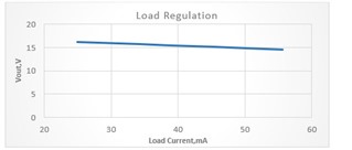
+15V output voltage load regulation rate
-5V output voltage load regulation rate
2) The power-on output voltage waveform of the converter
|
No-load startup waveform |
Fully loaded start-up waveform |
3) The voltage and current waveform of the SW pin:
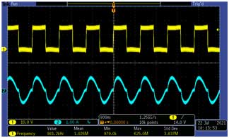
Figure 6 SW pin voltage and current waveform
Through the test results and experimental waveforms, it can be seen that the converter works in an under-resonant state, and maintains high efficiency and voltage accuracy when the input source is stable and the output power is 3.6W.
4 Supplement-Calculation of the driving power of the switch tube
The output power of the isolated power supply depends on the power required by the switch tube drive circuit. This part briefly supplements the calculation of the driving power required by the switch tube.
The driving of the switching tube is carried out by charging and discharging the gate (gate) junction capacitance of the switching tube through the driving voltage signal. For the calculation of drive power, the following formula can be used:
![]()
Among them, is the dynamic loss generated by the load switch; is the static loss of the isolated power supply in the output stage of the drive chip. Qg is the gate (gate) charge of the switching tube, which can be obtained in the specification; Vg is the pressure difference of the driving voltage, if +15V/-5V is used as the driving voltage of the switching tube, then Vg is 20V; fsw is the switch The operating frequency of the tube.
Take an IGBT (F3L300R12MT4_B22) as an example:
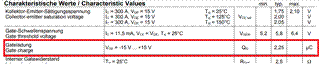
According to the data sheet, Qg is 2.25 µC, and the IGBT works at 10kHz. Aiming at the static loss of the output stage of the driver chip, take the single-channel isolated driver UCC5350 as an example, the specification ICC is 1.1mA, and the final drive power required is calculated as:
![]()
If the IGBT is used in a three-phase six-switch inverter, and a set of three-output isolated power supplies are designed to supply power to the isolated drive of the upper tube, the total output power of the designed isolated power supply should be greater than 1.416W (0.472W*3 ).


