
Shunlongwei Co. ltd.
IGBT Module / LCD Display Distributor
Customer Service
+86-755-8273 2562
IGBT Module / LCD Display Distributor
“The electric vehicle trend relies on the expected availability of electric vehicle (EV) charging infrastructure at public service stations, and can be accelerated by installing suitable charging systems in users’ homes and workplaces. While the core design requirements are largely the same, each system has specific requirements, compounded by regional differences in factors ranging from communication platforms to compliance requirements.
“
Author: Stephen Evanczuk
The electric vehicle trend relies on the expected availability of electric vehicle (EV) charging infrastructure at public service stations, and can be accelerated by installing suitable charging systems in users’ homes and workplaces. While the core design requirements are largely the same, each system has specific requirements, compounded by regional differences in factors ranging from communication platforms to compliance requirements.
The challenge for charging infrastructure designers is therefore to meet core requirements in a design that is flexible enough to meet the widest possible range of end applications and regional requirements, while balancing cost and time-to-market.
This article describes the design requirements for various public charging stations. It then introduces NXP Semiconductors’ flexible solution platform that can be used to develop designs that meet these requirements.
Meet diverse design challenges
Accelerating the transition to EV requires ready availability of efficient Electric Vehicle Supply Equipment (EVSE), better known as EV charging systems. Short-distance driving needs can be met with on-board AC-DC chargers built into the vehicle, which can be charged at home or office locations, but these charging systems do not alleviate EV range anxiety, which continues to limit EV adoption. Long-range EVs depend on the availability of public EV DC charging systems, which can charge EVs faster than built-in AC-DC chargers. At the same time, these different EV charging systems need to comply with multiple standards and regulations regarding safety, security and privacy.
For developers building EV charging system solutions, the need for effective solutions for each specific use case presents both enormous opportunities and significant technical challenges. Amid these challenges, developers need to provide a broad range of functionality across a range of designs that deliver the required performance and efficiency while meeting the specific requirements of each application. To meet this need, the fundamental architecture of all EV charging system designs needs to be adapted.
Adjusting the basic EV charging system architecture
Regardless of the specific target application, an EV charging system consists of two major subsystems—the power delivery front end and the power management back end controller; and are separated by an isolation boundary (Figure 1).
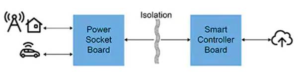
Figure 1: The basic architecture of an EV charging system consists of independent power outlet interfaces and controller subsystems separated by an isolation boundary. (Image credit: NXP Semiconductors)
On the vehicle and energy-oriented front end, the power outlet interface subsystem manages power delivery to the vehicle. On the other side of the isolation barrier, the controller subsystem handles safety, communications, and other advanced functions. The implementation of these subsystems often depends on some basic building blocks to meet the specific requirements of metering, control, functional safety, security and communications associated with each specific application.
Each building block provides key functions for the overall EV charging system design. Metering units need to ensure secure energy transmission, as well as accurate, tamper-proof energy measurements for billing purposes. The control unit ensures reliable execution of the various protocols required for downstream energy transmission and upstream data transmission. This unit is based on functional safety and security capabilities, while supporting local and region-specific requirements for secure payments and communication protocols used to communicate with cloud resources.
In the past, developers needed to implement every required building block, often using custom designs containing a variety of general-purpose components to adapt the basic EV charging architecture design as needed. NXP’s family of EV charging solutions provides an effective alternative, enabling developers to combine off-the-shelf building blocks to quickly create EV charging system designs to meet a wide range of target applications.
Implement EV charging system front end
At the heart of NXP’s EV charging solutions are families of processors designed to deliver the performance and functionality required for demanding applications such as EV charging system designs. Among these processor families, NXP’s Kinetis KM3x family of microcontroller (MCU) products are designed to provide certifiable and accurate power delivery measurements. Based on the Arm® 32-bit Cortex® M0+ core, Kinetis KM3x MCUs integrate a number of functional blocks for measurement, security, communication, and system support, as well as on-chip flash and static random access memory (SRAM) (Figure 2).
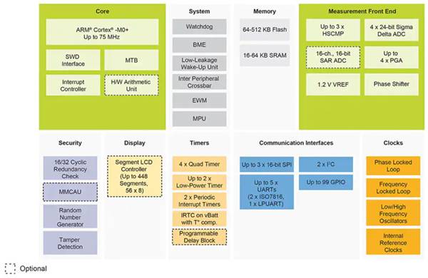
Figure 2: The Kinetis KM3x family integrates a complete set of required functional blocks to implement certifiable and accurate power delivery measurements. (Image credit: NXP Semiconductors)
To simplify metrology implementations, the KM35x MCU measurement front end integrates a high-precision delta-sigma analog-to-digital converter (ADC), multiple successive approximation register (SAR) ADCs, up to four programmable gain amplifiers (PGAs), a high-speed analog compare (HSCMP), a phase compensation logic block, and a high precision internal voltage reference (VREF) with low temperature drift. To protect the integrity of the unit of measure, on-chip security features support active and passive tamper detection with timestamps. Combined with external sensors, relays, and other peripherals, these on-chip function blocks provide all the functionality needed to quickly implement complex metering subsystems on the front end of an EV charging system power outlet (Figure 3).
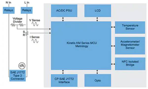
Figure 3: Using Kinetis KM MCUs, developers can implement an EV power outlet subsystem with only a few additional external components. (Image credit: NXP Semiconductors)
Implementing an EV Charging System Controller
As mentioned above, the EV charging system controller coordinates the various functions required by each system. The needs of this subsystem dictate the processor used to provide both the real-time performance that ensures precise control of the charging system, and the processing throughput to support a variety of protocols, while minimizing design footprint and cost.
Based on the Cortex-M7 core, NXP’s i.MX RT series of crossover processors provide the real-time capabilities of embedded microcontrollers and application processor-level performance. With an operating frequency of 600 MHz and a full set of peripherals, i.MX RT processors such as the i.MX RT1064 can meet the demands of low-latency real-time response. At the same time, features such as large on-chip memory, external memory controller, graphics subsystem, and a variety of connectivity interfaces also meet application needs (Figure 4).
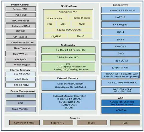
Figure 4: The i.MX RT1064 crossover processor combines peripherals and memory with an Arm Cortex-M7 processor subsystem designed to deliver real-time execution and application processor-level performance. (Image credit: NXP Semiconductors)
In addition to meeting critical real-time and performance requirements, EV charging systems need to be designed to ensure security in multiple areas, including power connection and payment method tamper detection and authentication. For data protection, secure boot, and secure debugging, developers can take advantage of the i.MX RT processor’s integrated security features, including high-assurance boot, hardware encryption, bus encryption, secure non-volatile storage, and a secure Joint Test Action Group ( JTAG) controller.
To further enhance the security of EV charging system controllers, designs typically incorporate NXP’s EdgeLock SE050 secure element to complement the i.MX RT processor’s security features. Designed to provide end-to-end lifecycle security, the SE050 provides hardware-based security accelerators for a range of common cryptographic algorithms, Trusted Platform Module (TPM) functions, secure bus transactions, and secure storage. By using the device to provide a root of trust (RoT) for the execution environment, developers can ensure the security of critical operations, including authentication, secure onboarding, integrity protection and attestation.
With i.MX RT processors and EdgeLock SE05x devices, developers can implement a controller subsystem to run a high-performance real-time operating system (RTOS) with only a few additional components (Figure 5).
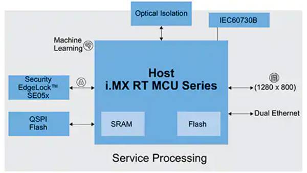
Figure 5: With integrated functional and performance capabilities, i.MX RT MCUs simplify the design of controller subsystems for EV charging systems. (Image credit: NXP Semiconductors)
Provides flexible solutions for different EV charging system applications
By combining the power and controller subsystems described above with optional payment and communication option blocks, developers can quickly implement single-phase EV charging systems capable of delivering up to 7 kW (Figure 6).
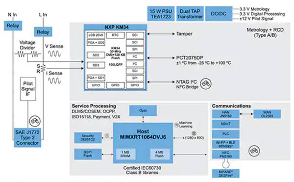
Figure 6: The KM3 MCU and i.MX RT crossover processor together provide an efficient hardware foundation for an EV charging system. (Image credit: NXP Semiconductors)
By slightly modifying the analog front end, the same design can be extended into a three-phase EV charging system capable of delivering up to 22 kW (Figure 7).
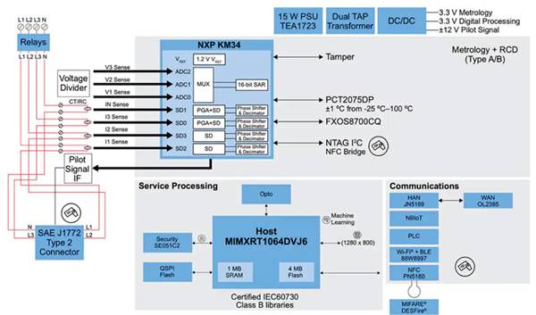
Figure 7: Developers can quickly adapt a KM3 MCU and i.MX RT crossover processor-based design to support a variety of applications. (Image credit: NXP Semiconductors)
While this combination of KM3x and i.MX RT devices is suitable for many use cases, other EV charging system applications may require developers to optimize other aspects of their designs. For example, residential chargers are designed to provide faster charging times than on-board chargers, so solutions that optimize their cost and footprint are needed. For these applications, developers can use cost-effective MCUs such as NXP’s LPC55S69 to implement lower-cost entry-level controllers.
In contrast, commercial EVSE chargers for public service stations will place more stringent requirements on high-speed application processing and real-time performance. For battery storage systems operating at 400 to 1000 V and providing a charge level of 350 kW or higher, the above requirements are required for safe system control. Among them, the ability to execute application-level software and real-time software is critical to performance and functionality. For these systems, using products such as NXP’s i.MX 8M processors, developers can more easily implement charging solutions that provide the Linux-based application processing and RTOS-enabled real-time performance required for these complex designs ( Figure 8).
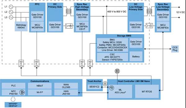
Figure 8: For more complex applications such as ultra-high-speed EV charging, developers can extend the basic EV charging architecture with high-performance processors such as the i.MX 8M processor to support more complex controller requirements. (Image credit: NXP Semiconductors)
Rapid implementation of cloud-connected EV charging systems
NXP processors include Kinetis KM3x, i.MX RT, LPC55S69 and i.MX 8M, providing a flexible platform to meet the specific requirements of different EV charging system applications. However, for more complex applications, delays in the deployment of hardware infrastructure can cause significant delays in the development of end-to-end EV charging system applications.
To avoid this delay, NXP offers a rapid development path using a set of boards and evaluation kits based on the aforementioned devices. For example, NXP’s TWR-KM34Z75M module provides a complete metrology platform that combines the KinetisMKM34Z256VLQ7 metrology MCU and a full suite of supporting components. Likewise, NXP’s i.MX RT1064 evaluation kit combines the MIMXRT1064DVL6 processor with 256 Mb SDRAM, 512 Mb Flash, 64 Mb Quad SPI (QSPI) Flash on a four-layer board with a rich set of peripheral connections device, including an Arduino interface. Additionally, NXP’s OM-SE050ARD board provides ready access to the EdgeLock SE050, while NXP’s PNEV5180BM evaluation board provides a ready-to-use NFC front-end development board.
By combining NXP’s TWR-KM34Z75M board for metering, i.MX RT1064 for control, and the OM-SE050ARD and PNEV5180B boards, developers can quickly implement a full-featured hardware platform to build EV charging system applications (Figure 9).
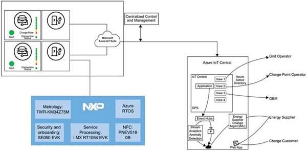
Figure 9: Using NXP boards and evaluation kits, developers can quickly implement a complete end-to-end EV charging solution through available cloud services such as Microsoft Azure. (Image credit: NXP Semiconductors)
The combination of NXP’s board-level solutions and Microsoft Azure cloud services enables developers to rapidly prototype complete end-to-end EV charging system solutions and use the platform as a foundation to design more specialized applications.
Summarize
The ready availability of EV charging systems is a key enabler for electric vehicles, but it remains a hindrance to cost-effectively implement the different solutions required in homes, offices and public service stations. Leveraging NXP Semiconductors’ dedicated device and board solutions platform, developers can quickly implement designs that perform well for all EV charging applications, with the flexibility to adapt to emerging requirements.
The Links: DMF50840-NB-FW G070VW01-V0


