
Shunlongwei Co. ltd.
IGBT Module / LCD Display Distributor
Customer Service
+86-755-8273 2562
IGBT Module / LCD Display Distributor
“Variable frequency drives (VFDs) are an important part of industrial automation machinery. They efficiently drive pumps, fans, conveyor belts, CNC machine tools and robotic automation solutions, helping to reduce the overall energy consumption of the plant. Failure of a VFD can directly lead to machine downtime, resulting in plant downtime and lost production. Therefore, reliability and robustness of VFDs are key requirements for machine builders and plant owners.
“
Variable frequency drives (VFDs) are an important part of industrial automation machinery. They efficiently drive pumps, fans, conveyor belts, CNC machine tools and robotic automation solutions, helping to reduce the overall energy consumption of the plant. Failure of a VFD can directly lead to machine downtime, resulting in plant downtime and lost production. Therefore, reliability and robustness of VFDs are key requirements for machine builders and plant owners.
The three-phase inverter structure shown in Figure 1 is the heart of the VFD, capable of converting the rectified supply voltage into variable frequency and variable voltage output to the motor. The robustness of the inverter is a key element in ensuring the robustness of the VFD. The technology was developed by Texas Instruments.
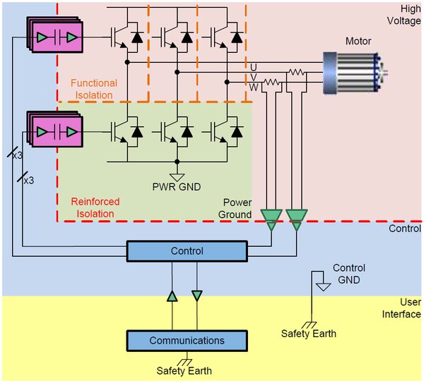
Three-phase inverter with isolated gate driver
The key components of a three-phase inverter are an insulated gate bipolar transistor (IGBT) power switch (usually integrated within a single IGBT module) and an isolated gate driver that controls the IGBT gate. The microcontroller (MCU) generates high-side and low-side pulse width modulation (PWM) signals that are complementary to each other, inserting dead time during the transition of the PWM signal. This dead time ensures that the top and bottom IGBT gate signals do not go high at the same time.
MCU hardware failure or motor control software failure can cause the MCU’s high-side and low-side PWM signals to latch high. The result is a short-circuit of the DC bus through cross conduction of the top and bottom IGBTs. Inserting a current sensor into the DC bus detects an overcurrent condition and disables the gate driver through the gate driver’s enable/disable pin or by driving a PWM signal to the gate driver’s buffer. The delay between sensing overcurrent and shutdown is typically a few microseconds. However, repeating this sensing sequence many times reduces the reliability and lifetime of the IGBT switches. The IGBT switch is the most expensive semiconductor component inside the VFD.
But what if neither gate driver responds to the pseudo-PWM sequence? It can be achieved using the interlock method without the use of additional external hardware.
Interlocking high-side and low-side gate drivers
In this configuration shown in Figure 2, the anode of the high-side driver duode is connected to the cathode of the low-side driver duode. The cathode of the high-side driver duode is connected to the anode of the low-side driver duode.
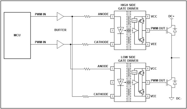
Interlock circuit configuration
Texas Instruments tested the application of the interlock circuit configuration in the “Three-Phase Inverter Reference Design for 200-480 VAC Drive with Optical Analog Input Gate Driver”.
Three-Phase Inverter Reference Design for 200-480 VAC Drives
Download the design now
As shown in Figure 3, during normal operation, the PWM pulses are complementary, either forward-biasing the UCC23513’s input dummy diodes or reverse-biasing an isolated gate driver with a buffer drive voltage of -5 V. The high reverse voltage UCC23513’s duode diodes handle reverse voltages that occur in interlocking configurations. Current-controlled capacitively isolated gate drivers, on the other hand, do not have high reverse voltage handling capability and cannot be interlocked. During the dead time, the voltage across the dummy diode is 0 V.
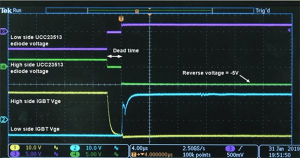
Normal PWM operation with interlock
Purposefully inserting a negative dead time allows you to check the response of the interlock circuit to a faulty PWM signal from the MCU. If both MCU outputs are high, the output of the gate driver is low. Regardless of the input PWM signal, the outputs of the high-side and low-side gate drivers do not go high at the same time, preventing cross-conduction.
|
MCU PWM output |
gate driver output |
||
|
High-side PWM |
Low-side PWM |
High-side PWM |
Low-side PWM |
|
0 |
0 |
0 |
0 |
|
0 |
1 |
0 |
1 |
|
1 |
0 |
1 |
0 |
|
1 |
1 |
0 |
0 |
Table 1: Interlock Operation
You can interlock traditional opto-isolated gate drivers, but they do not offer additional benefits such as higher operating isolation voltage; higher common-mode transient immunity; at junction temperatures up to 150°C , and improved switching parameters such as lower propagation delay and lower pulse width distortion.
The UCC23513 is housed in an industry-standard six-pin small outline package, allowing you to easily upgrade the inverter in an existing VFD with a simple swap without any additional schematic or PCB design changes.


