
Shunlongwei Co. ltd.
IGBT Module / LCD Display Distributor
Customer Service
+86-755-8273 2562
IGBT Module / LCD Display Distributor
“Integrated passive devices are nothing new in our industry-they are long-established and well-known. In fact, ADI has produced such components for the market in the past. When the chipset includes independent discrete passive components or integrated passive networks as part of it, careful design management is required for considerations such as trace parasitics, device compatibility, and Circuit board assembly. Although integrated passive devices continue to occupy an important position in the industry, their most important value can only be realized when they are integrated into system-in-package applications.
“
Introduction
Integrated passive devices are nothing new in our industry-they are long-established and well-known. In fact, ADI has produced such components for the market in the past. When the chipset includes independent discrete passive components or integrated passive networks as part of it, careful design management is required for considerations such as trace parasitics, device compatibility, and circuit board assembly. Although integrated passive devices continue to occupy an important position in the industry, their most important value can only be realized when they are integrated into system-in-package applications.
A few years ago, ADI began to launch a new integrated passive technology program (iPassives?). ADI aims to provide passive components such as diodes, resistors, inductors, and capacitors through this program, which can cover signal chain design more widely, while overcoming the limitations and complexity of existing methods using passive components. The demand of ADI’s customer base for more complete solutions with efficient space dimensions has also promoted the development of this program. From the designer’s point of view, iPassives can be regarded as a flexible design tool that can design system solutions with best-in-class performance and robustness in a very short development cycle. ADI has many signal conditioning ICs, and our unique silicon manufacturing process enables these ICs to achieve excellent performance. ADI can make full use of the diversity of its existing products to produce plug-and-play systems with outstanding performance characteristics without the need to develop highly complex integration processes. Closely integrate integrated passive technology with all these existing technologies in a highly customizable network, and use system-in-package technology for packaging to create a fully certified, tested, and characterized μModule? Device. Systems that previously used board-level solutions can now be reduced to a single device. From the perspective of our customers, they can now get a complete solution with excellent out-of-the-box performance, shorten the development cycle and save costs, all of which are implemented in a very compact package.
Passive technology
Now, let’s briefly review the basics and recall what passive components are. Passive components are devices that do not require power supply, and the relationship between their current and voltage is relatively simple. These components include resistors, capacitors, inductors, transformers (that is, effectively coupled inductors), and diodes. Sometimes the relationship between current and voltage is very simple, just as the current in a resistor changes linearly with voltage. For diodes, there is also a direct relationship between current and voltage, but this relationship is exponential. In inductance and capacitance, the relationship is the transient dependence of current on voltage. Table 1 shows the formulas that define these relationships for four basic passive components:
Table 1.Basic formula for main passive components
Discrete components
formula
symbol
resistance
![]()
![]()
V = voltage
I = current
t = time
R = resistance (ohm)
C=Capacitance (Farad)
L = coil inductance (Henry)
IS = diode saturation current
VT = thermal voltage
h = diode ideality factor
capacitance
![]()
![]()
inductance
![]()
![]()
diode

![]()
Passive components can be used alone, or in series or parallel. They are analog signal processing (RLC is used for amplification, attenuation, coupling, tuning and filtering), digital signal processing (pull-up resistors, pull-down resistors and impedance matching resistors), EMI An important part of suppression (LC noise suppression) and power management (R is used for current detection and limitation, and LC is used for energy accumulation).
Limitations of discrete components
In the past, passive components were discrete, which meant that they were manufactured separately and connected in the circuit by wires or power rails on a printed circuit board (PCB). Over time, they have evolved along three paths: smaller size, lower cost, and higher performance. These developments are now very mature and optimized, but the footprint and height dimensions mean that discrete passive components always limit the effectiveness of efforts to reduce the area and volume of the overall solution. Passive devices usually account for more than 80% of the bill of materials in an application, about 60% of the circuit board area, and about 20% of the entire component expenditure. These factors combine to create very complex inventory control and storage challenges.
In its essence, discrete devices are individually processed components. Although there may be ways to ensure that components are selected from certain process batches, each component is still highly unique. However, when very matched components are required, this is a significant disadvantage. For devices that need to be matched, the uniqueness and differences between components will cause errors, thereby reducing the circuit performance at time zero. In addition, this kind of performance degradation is always getting worse during the operating temperature range and service life of the circuit.
Another disadvantage of discrete passive devices is that the assembly and wiring of individual components is very time-consuming and also takes up a lot of space. These components are connected using a soldering process, which is generally assembled through through-hole or surface mount packaging technology (SMT). Through hole is an older assembly technology. It inserts a component with a lead into a hole in the PCB. Any excess lead length will be bent and cut off, and the lead of the component is connected to the PCB interconnection power supply by wave soldering. rail. Surface mount packages help realize smaller passive components. In this case, etch and mount the connection pattern on the PCB, cover the pattern with solder paste, and then use the placement machine to position and place the SMT components. Then, the PCB undergoes a reflow soldering process (in which the solder paste is liquefied and an electrical connection is established), and when cooled, the solder paste solidifies and mechanically connects the SMT components to the PCB. The main problem with these two assembly technologies is that the welding process can be very unreliable, which is increasingly worrying in industries where the defect target is a few parts per million. There are several factors that are very important in ensuring the reliability of solder joints: the actual composition of the solder paste (now basically lead-free, so the reliability is reduced), the mechanical stability of the reflow soldering process (mechanical vibration can make the solder joints Drying), the purity of the solder paste (any contaminants will have a negative impact on the reliability of the solder joint), and the time and temperature of the reflow soldering process. The speed at which the solder paste is heated, the actual temperature and temperature uniformity, and the time during which the solder paste is heated are all critical. Any of these changes may cause damage to the connection pads or vias, or may also cause mechanical stress on the device, leading to failure over time.
Another limitation of using passive components on the PCB is that the traces need to be very long because they are distributed everywhere on the board. This may introduce unaccounted parasitic parameters, which limits the repeatability of performance and results. Generally, PCB traces have a self-inductance length and capacitance of about 1 nH/mm, depending on the line width and the distance from nearby traces. The tolerance of PCB trace leads to the variation of parasitic parameters, so not only does it bring the destructive effects of parasitic effects, but they are also unpredictable. Narrowing tolerances on the PCB will increase cost.
Passive devices also provide many potential contact points with the outside world. These contact points may cause ESD events after manual or machine processing. Again, this will have adverse effects and risks on overall reliability and robustness.
Advantages of integrated passive components
Before delving into the advantages of integrated passive devices over discrete passive devices, let’s first outline the origin of integrated passive devices. Integrated Circuits now contain many transistors (in fact, millions), which are connected to each other by fine metal. For analog applications, the industry has also developed special processes. For example, DACs and ADCs include passive components such as resistors and capacitors in addition to transistors. In order to achieve the performance required for these sophisticated analog applications, very high-quality passive components have been developed. It is these high-quality passive components that are used to build integrated passive devices. Just as an integrated circuit contains many transistors, integrated passive devices can contain many high-quality passive components in a very small package. Like integrated circuits, integrated passive devices are fabricated on a large-area substrate (wafer) to generate multiple passive networks at the same time.
Compared with discrete passive components, one of the most noticeable advantages of integrated passive components is that they can achieve precise matching. When manufacturing an integrated passive network, all components in the network are manufactured at the same time under the same conditions, with the same materials, and because the network is compact, they are basically at the same location. Passive components manufactured in this way are more likely to have excellent matching than discrete passive components. To illustrate this point, we assume that there is an application that requires two matched resistors. These resistors are fabricated on a circular substrate (such as a silicon wafer), as shown in Figure 1. Due to subtle process differences, such as the thickness of the resistive film, the chemical properties of the film, contact resistance, etc., there will be a certain resistance difference in the same batch, and the difference is greater in multiple batches. In the example shown in Figure 1, dark green indicates that the resistor is at the high end of the tolerance range, and yellow indicates that the resistor is at the low end of the tolerance range. For standard discrete devices, any of the two resistors may come from different manufacturing batches, such as the two separate resistors shown in red in the figure. The observable tolerance range between these two discrete resistors may be the tolerance range of the entire process, so the matching is poor. For special ordering restrictions, it is possible to select these two discrete resistors from the same batch, as shown in the figure with two separate resistors marked in blue. The observable tolerance between these two resistors will only be the tolerance range within the same batch. Although the matching between these two resistors will be better than the case of random discrete devices, there may still be some degree of mismatch. Finally, for integrated passive devices, the two resistors come from the same chip, as shown in black in Figure 1. The only observable tolerance between these two resistors is the tolerance range within the same die. Therefore, the matching between these two resistors will be excellent. In addition, other technologies and other methods using cross quadrilateral layout can further strictly limit the diffusion between the two resistors, so that the matching of the components can reach the best value. The matching between integrated passive components is not only much better than discrete passive components at the time zero point, but also because its manufacturing has been well coupled, so it can maintain a better match over the entire temperature, mechanical stress and service life range record.
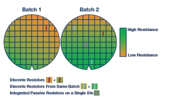
figure 1. The matching comparison of discrete resistance and passive resistance.
The various components in the integrated passive device are placed closely together (actually in the micrometer range), so interconnection parasitic parameters (such as wiring resistance and inductance) can be kept at an extremely low level. On the PCB, due to trace tolerances and component placement tolerances, interconnect parasitic parameters may change. Because the lithography process is used in the manufacturing process, the interconnect tolerance and component placement tolerance of using integrated passive devices are very small. In integrated passive devices, not only the parasitic parameters are very small, but these few parameters are still predictable, so the reliability is very high.
The miniaturization of passive networks by integrating passive components directly brings the advantages of small size to the circuit board. This directly reduces the cost of the circuit board and allows more functions and higher performance to be implemented in a smaller footprint. When using integrated passive components, building a multi-channel system becomes more practical and feasible.
Another significant advantage of integrated passive devices is the robustness around the entire wiring network. Integrated passive components are essentially forged together in a complete unit, sealed with glass, and then further protected by a strong plastic package, without the need for a large number of solder connections. In the integrated passive network, there is no problem of dry solder joints, corrosion or component misalignment.
Another advantage brought by the excellent sealing performance of the integrated passive network is that the number of exposed nodes in the system is greatly reduced. Therefore, the possibility of system damage due to accidental short circuits or electrostatic discharge (ESD) events is significantly reduced.
Maintaining and controlling the component inventory of any circuit board assembly is a very complex task. Integrated passive components include multiple passive components in one device, which greatly reduces the burden on customers’ bills of materials, thereby reducing the cost of ownership. Customers can get a fully tested and fully validated integrated passive network. This means that the output of the final circuit board construction is increased, which not only can further save costs, but also improve the predictability of the supply chain.
Use ADI’s integrated passive components (iPassives)
As mentioned earlier, high-quality passive components have always been the core of the circuit performance achieved by ADI’s many products over the years. During this period, the range of passive devices continued to expand and the quality continued to improve, and the integrated passive device product portfolio now contains a large number of components. Integrated passive devices use a modular process, which means that the process steps required to produce a certain type of passive device need to be performed only when specific components are needed. The construction of the iPassives network basically only requires the necessary process complexity, no more, no less. As shown in Figure 2, there are many passive building blocks to choose from, and building an integrated passive network is as simple as putting together the required components.
figure 2. iPassives building blocks.
As mentioned earlier in this article, integrated passive devices have many advantages over discrete passive devices. ADI uses them in μModule devices to further strengthen these advantages. These Modules take advantage of the functions of various integrated circuits. These circuits are manufactured through tailor-made processes, and the enhanced performance provided by them cannot be achieved by any other single process. ADI is using iPassives to connect these integrated circuits together, thereby building a complete precision signal chain within a single device. The two μModule device examples in Figure 3 include data converters, amplifiers, and other components, which are combined by passive gain and filter networks constructed with integrated passive components.
image 3. Examples of μModule products using iPassives.
ADI produces highly customizable precision signal conditioning systems. Using a reusable approach from a large portfolio of field-proven IC products and combining it with the versatility of iPassives, the development cycle time and cost are significantly reduced. This decision provides customers with a huge advantage, enabling them to use the most advanced capabilities to enter the market faster and more efficiently.
in conclusion
At first glance, the use of integrated passive components may only appear slightly more advantageous than other more mature methods. However, the actual advantages are more significant. ADI uses iPassives to not only redefine the achievable functions, but also redefine the speed, cost and design size, making it more beneficial to customers.
The Links: TPS65251RHAR G121SN01-V403


