
Shunlongwei Co. ltd.
IGBT Module / LCD Display Distributor
Customer Service
+86-755-8273 2562
IGBT Module / LCD Display Distributor
Called PSC1065K, the company is not making its full data sheet public – the data brief reveals 15nC total capacitive charge (Vr=400V, 200A/μs, Tj=150°C), but not forward voltage.
It is one of the company’s ‘merged PiN Schottky’ diodes.
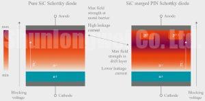
“Imperfections at the metal-semiconductor interface are responsible for leakage currents in SiC Schottky diodes,” according to the company. “While these can be reduced by using a thicker drift layer, it comes with the disadvantage of higher ohmic and thermal resistance.”
The merged structure, “effectively combines a Schottky diode and a p-n diode connected in parallel”, it explained. “p-doped areas are implanted in the drift zone of a conventional Schottky structure, forming a p-ohmic contact with the metal at the Schottky anode and a p-n junction with the lightly-doped SiC drift or epi-layer.”
Under reverse bias, the p-wells push the general area of maximum field strength downwards into the “almost defect-free” drift layer, it said, away from the metal barrier with its imperfections, reducing the overall leakage current.
The p-well’s placement and area compared with the size of the Schottky diode, and doping concentration, affect the end characteristics, with forward voltage drop traded against leakage and surge currents.
“As a result, an MPS device can operate at a higher breakdown voltage with the same leakage current and drift layer thickness,” said Nexperia.
In the pipeline are similar devices in the larger TO-247-2 through-hole package, as well as DPAK R2P and D2PAK R2P surface mount versions, then automotive-grade 650V and 1.2kV parts.
Applications are foreseen in battery-charging, uninterruptible power supplies and photovoltaic inverters.
View more : IGBT modules | LCD displays | electronic components
