MOSFET and IGBT Technologies
MOSFETs can switch at higher frequencies due to the absence of minority carrier transfer. The limitations are determined by two factors: the transit time for electrons to cross the drift region and the time required to charge and discharge the input gate and Miller capacitance.
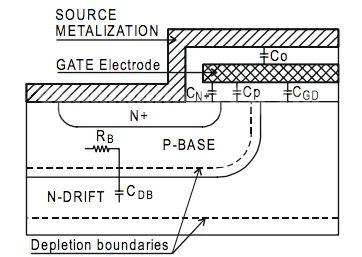
IGBT combines the advantages of MOSFET and BJT. It operates like a MOSFET but has an injection region on its drain side to modulate the conductivity of the drain drift region, reducing conduction losses, especially compared to high-voltage MOSFETs with equivalent ratings.
Regarding IGBT drive, it is similar to MOSFETs, so all the annotations, charts, and driver circuits designed for driving MOSFETs are equally applicable to IGBTs. Therefore, the following discussion focuses on the MOSFET model.
Integrated Circuit Drivers
While there are various methods to drive MOSFET/IGBT using hardwired electronic circuits, the convenience and functionality offered by IC drivers have attracted designers. The key advantage is compactness. IC drivers inherently provide lower propagation delay. Since all critical parameters are specified within the IC driver, designers do not need to go through the time-consuming process of defining, designing, and testing circuits to drive MOSFET/IGBT.
Techniques for Increasing Current Output
The totem-pole configuration with N-channel and P-channel MOSFETs can be used to boost the output of IC drivers. The drawback is signal inversion, and there is a risk of breakdown during common gate voltage transitions.
Using Charge Pumps and Bootstrap Techniques
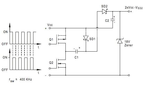
To drive the upper MOSFET/IGBT in bridge topologies, buck converters, or 2-transistor forward converters, low-side drivers cannot be used directly. This is because the source/emitter of the upper MOSFET/IGBT is not at ground potential.
Figure 2 shows how a charge pump creates a higher Vcc for the driver IC of the upper MOSFET/IGBT. Here, a pair of N-channel and P-channel MOSFETs act as switches, alternately connecting the input power supply voltage to the output through capacitors and Schottky diodes, isolating it and almost doubling it. With a switching frequency in the hundreds of kHz, the low-ripple isolated output voltage serves as the DC source for driving the upper MOSFET/IGBT.
Practical Considerations
Several practical issues must be taken into account when designing and constructing MOSFET/IGBT driver circuits to avoid unpleasant voltage spikes, ringing oscillations, and false turn-ons. These problems typically arise from improper or insufficient power supply bypassing, layout, and mismatches between the driver and the driven MOSFET/IGBT.