
Shunlongwei Co. ltd.
IGBT Module / LCD Display Distributor
Customer Service
+86-755-8273 2562
IGBT Module / LCD Display Distributor
The presence of undesired electronic noise in semiconductors has the potential to be used in many applications. However, it is important to note that such applications are generally not preferred, as electronic noise is commonly seen as a disadvantageous factor that negatively impacts the performance of semiconductor devices. Nevertheless, certain instances have demonstrated that researchers and engineers have managed to utilize or manipulate electronic noise for certain objectives.
This article draws from a recent discovery made by a group of researchers from the Center for Integrated Nanostructure Physics within the Institute for Basic Science (IBS), South Korea. The researchers have made a breakthrough in utilizing the fluctuations and electronic noise in semiconductors intentionally created by introducing vanadium in a properly layered semiconductor.
Even though the primary focus in semiconductor technology is typically on minimizing and controlling noise to enhance device performance and reliability, some potential applications of electronic noise are meaningful, such as:
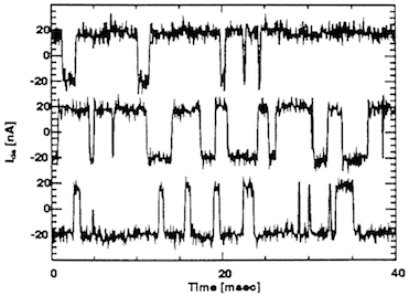
A form of electronic noise that is typically found in semiconductor devices, especially MOSFETs (Metal-Oxide-Semiconductor Field-Effect Transistors) and other nanoscale transistors, is Random Telegraph Noise (RTN). RTN, also known as Burst noise, is characterized by random and abrupt switching between discrete levels of current as shown in Figure 1. It is caused by the localized capture and release of individual charge carriers (electrons or holes) within the semiconductor material or at the semiconductor-dielectric interface. This process of capturing and releasing causes fluctuations in the transistor’s current over time.
RTN can have substantial effects on the performance and dependability of semiconductor devices, especially as transistor sizes shrink and device dimensions near the nanometer scale. Variations in device characteristics such as threshold voltage, subthreshold slope, and discharge current can affect the precision and stability of electronic circuits.
Besides defect characterization, RTN can provide valuable insights into the device reliability assessment. Here, RTN can serve as an indicator of the semiconductor device’s long-term reliability. It can be used to evaluate the stability and deterioration of devices over time. Observing how RTN characteristics change under various operating conditions can aid manufacturers in predicting the product’s lifespan and potential failure modes.
What the researchers have discovered is a potential application of unwanted electronic noise, such as RTN, in semiconductors. The team, which was led by Professor LEE Young Hee, demonstrated that magnetic fluctuations and the enormous RTN signals that they produce may be created in a vdW-layered semiconductor by inserting vanadium in tungsten diselenide (V-WSe2) as a minute magnetic dopant. The research was published in the journal Nature Communications.
Tungsten diselenide is a compound consisting of tungsten (W) and selenium (Se) atoms arranged in a specific crystal lattice structure. It belongs to a class of materials known as transition metal dichalcogenides (TMDs), which have gained significant attention in recent years due to their unique electronic, optical, and mechanical properties. TMDs like tungsten diselenide are two-dimensional materials, meaning they are composed of atom-thin layers with strong covalent bonds within the layers but weak van der Waals forces between the layers.
Tungsten diselenide has some interesting properties, including:
Random telegraph noise is most frequently brought on by two-state defects in semiconductors. When compared to their three-dimensional (3D) counterparts, two-dimensional (2D) van der Waals (vdW) layered magnetic materials are expected to display huge fluctuations due to long-range Coulomb interaction. More importantly, these fluctuations might be controlled by a voltage, which is a significant advantage over the 3D counterparts’ large charge screening.
Researchers used vertical magnetic tunneling junction devices to study multilayered vanadium-doped tungsten diselenide (WSe2), and they found that the material exhibited electrically controllable magnetic fluctuations and an RTN signal.
In lateral devices, the high contact resistance typically inhibits the manifestation of quantum states and degrades the performance of the device itself. For this reason, the researchers introduced a vertical magnetic tunneling junction device by sandwiching several layers of the magnetic material V-WSe2 between the top and bottom graphene electrodes. Even with a modest vanadium doping concentration of 0.2%, this vertical magnetic tunneling junction device was able to demonstrate quantum states such as magnetic fluctuations and produce RTN signals with high amplitude.
The researchers detected RTNs with a high amplitude of up to 80% between well-defined two-stable states while carrying out the resistance measuring studies utilizing these devices. Because of the struggle between intralayer and interlayer coupling among the magnetic domains, the bistable state is characterized by magnetic variations in resistance that increase with temperature. They were able to determine the identity of this bistable magnetic state by looking for discrete Gaussian peaks in the RTN histogram in conjunction with specific characteristics in the noise power spectrum.
The most crucial thing that the researchers found was that they were able to change the cut-off frequency of the RTN as well as the bistable magnetic state of the RTN simply by switching the polarity of the voltage. This remarkable finding paves the path for the application of 1/f2 noise spectroscopy in magnetic semiconductors and offers the possibility of magnetic switching in spintronics.
Figure 2 shows the time evolution of RTN signals along with the RTN histograms of the 1/f2 feature in the noise power spectra at negative (a) and positive (b) voltages. In the 1/f2 histogram, the high-resistance state corresponds to antiparallel spin states between layers (a) and the low-resistance state corresponds to parallel spin states between layers (b).


