Content last revised on September 17, 2026
Assembly Integrity and Isolation Verification for 2SC0108T2A0-17
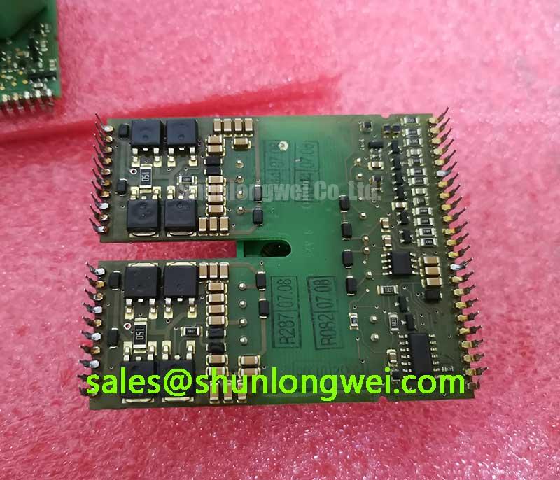
Before fitting a 2SC0108T2A0-17 into a replacement inverter control assembly, isolate the equipment, inspect the driver connection area for heat discoloration or contamination, and verify that the control-side and power-side wiring paths remain physically separated. This Power Integrations Concept IGBT gate driver has an official 4 kVAC test voltage for 1 minute, providing galvanic isolation between the low-voltage control domain and the high-voltage power domain.
The official device information states compatibility with IGBTs rated up to 1700 V. That voltage figure is an IGBT blocking-voltage compatibility boundary, not a declared DC-link operating voltage or an instruction for insulation coordination. The system integrator should verify the complete power-stage voltage, the original IGBT module rating, creepage distances, enclosure contamination level, and applicable safety requirements from the equipment documentation.
Galvanic isolation prevents a direct conductive path between the control electronics and the power section while allowing gate-drive commands to cross the boundary. The practical function of this arrangement is described in Galvanic Isolation Principles in High Voltage Power Systems. In field service, do not treat an isolation test-voltage rating as proof that every surrounding PCB material, cable, connector, or auxiliary supply channel meets the same insulation capability.
Design Consideration: maintain the separation established by the original equipment layout when replacing the driver or repairing nearby PCB damage. Added jumper wires, residue around isolation slots, and rerouted auxiliary-supply wiring can alter the intended return paths and increase sensitivity to switching noise. Where an oscilloscope shows an unexplained gate pulse, compare the command input, isolated supply behavior, and gate output with a known-good channel before attributing the symptom to one component.
For commercial string inverter or micro-grid energy-storage equipment, this driver can be evaluated as part of an IGBT power-stage repair only after confirming the original channel count, interface logic, isolated supply arrangement, connector orientation, and protection architecture. A gate driver cannot be selected from IGBT voltage class alone.
2SC0108T2A0-17 Gate Loop Control and Switching Coordination
The ±8 A peak gate-current capability is an Official Datasheet Specification for the 2SC0108T2A0-17. It describes the output stage’s ability to source and sink gate current for charging and discharging the connected IGBT gate capacitance. Actual switching behavior remains dependent on the IGBT gate-charge characteristic, external gate network, PCB geometry, DC-link construction, temperature, and the operating current of the finished converter.
The official typical propagation delay is approximately 80 ns. This supports timing analysis between the input command and output response, but it must not be used alone to establish a complementary-switch dead-time value. Design Consideration: interlock behavior, driver-channel delay variation, IGBT switching characteristics, and the measured commutation waveform should be reviewed together. The system engineer must validate peak voltage and current margins during switching tests under the intended operating conditions.
Keep the power emitter path distinct from the gate-drive return arrangement specified by the original IGBT module and driver implementation. Shared high-current return impedance can couple switching current into the gate reference and may contribute to ringing, uneven switching, or false transitions. Short, direct gate-loop routing and preservation of the original return topology are practical measures when repairing a failed inverter gate-drive board.
Reverse recovery of the complementary freewheel diode can also influence the observed switching transient. Its softness factor and the surrounding commutation-loop inductance affect the current transition and radiated noise behavior, but neither is an official specification published here for the 2SC0108T2A0-17. Engineering Recommendation: use measured gate-emitter voltage, collector-emitter voltage, and current waveforms to assess the assembled power stage rather than inferring diode behavior from the gate-driver rating.
Long motor cables can introduce transmission-line reflections that increase stress at the motor terminals. That phenomenon belongs to the complete inverter, cable, motor, filtering, and grounding system. When such equipment is being repaired, verify the original output filtering and cable arrangement rather than attempting to correct a motor-side waveform by changing driver settings without controlled validation.
2SC0108T2A0-17 Installation Inspection and Thermal Maintenance Boundaries
The 2SC0108T2A0-17 is a gate driver, not an IGBT power module or a baseplate-mounted thermal interface component. No official thickness requirement for thermal interface material, heatsink flatness, mounting screw torque, or baseplate curvature is provided for this driver in the supplied factory specifications. Those parameters must therefore be taken from the original equipment assembly documentation and from the documentation for the associated IGBT module.
During preventive maintenance, inspect the inverter cooling path, heatsink cleanliness, fan operation, electrical terminals, and any thermal interface material used beneath the actual power module. Deteriorated thermal contact in the IGBT assembly can raise switching-device temperature and alter the operating conditions seen by the gate-drive system. This does not establish a fault in the 2SC0108T2A0-17; it identifies a system condition requiring inspection.
Maintenance Note: De-energize the equipment and confirm the DC link is safely discharged before disconnecting driver, gate, or auxiliary-supply connections.
Design Consideration: where a board-mounted driver is located near a hot power stage, inspect for dust accumulation, moisture exposure, connector fretting, cracked solder joints, and discoloration around isolated supply components. In high-humidity or large temperature-swing environments, confirm that the enclosure and maintenance practice prevent condensation from bridging control-side and power-side conductors.
When a repair requires evaluation of the associated IGBT module, SKM75GB07E3 is a separately listed IGBT module that can be reviewed against the original unit’s electrical, mechanical, and gate-drive requirements. It is not an asserted replacement for any existing assembly; compatibility must be confirmed from the equipment design and original component documentation.
2SC0108T2A0-17 Protection Verification and Reliability Checks
Start a protection-related investigation by checking whether the driver input command, isolated supply condition, gate output, IGBT gate-emitter waveform, and controller fault response agree with the known circuit sequence. The 2SC0108T2A0-17 provides the stated output-current, propagation-delay, isolation-test-voltage, and IGBT blocking-voltage compatibility parameters, but the supplied specifications do not establish a complete converter protection threshold, short-circuit withstand time, or fuse coordination value.
Fast semiconductor fuses are selected within the complete power-stage protection design using device energy limits, prospective fault current, interruption behavior, conductor layout, and the protection coordination defined by the equipment manufacturer. A fuse I²t value cannot be derived from the driver’s ±8 A gate-current rating. Likewise, a driver-output measurement does not by itself prove that an IGBT has survived a short-circuit event.
Heavy pulsed operation produces transient heating in the power semiconductor. Calculation of junction-to-case response can use a multi-RC thermal model only when the associated IGBT module’s official transient thermal data, pulse profile, case condition, and initial temperature are known. Engineering Calculation based on those inputs may support a temperature-margin assessment, but no such thermal model or junction-temperature specification is claimed here for the 2SC0108T2A0-17.
For a disciplined inspection sequence, first compare static resistance checks with the original service procedure, then examine waveform timing at low-risk commissioning conditions, and finally verify the full protection chain under controlled test conditions. Unstable gate behavior may indicate an input-signal issue, auxiliary-supply disturbance, grounding problem, connector fault, layout-related coupling, or a damaged power device. A waveform comparison against a verified operating channel provides more useful evidence than a single resistance reading.
For system-level discussion of isolation, gate-loop behavior, switching validation, and measurement discipline, see Precision Gate Drive Design. The final integration decision remains system-determined and should be verified against the original power-stage documentation.