
Shunlongwei Co. ltd.
IGBT Module / LCD Display Distributor
Customer Service
+86-755-8273 2562
IGBT Module / LCD Display Distributor
“The rapid development of Electronic information technology has promoted the rapid progress in the field of power supply technology, and has also brought unprecedented opportunities and challenges to power supply engineers and technicians, ranging from household appliances to large-scale instruments and equipment used in the power industry. Power supply to provide energy, which also requires a large number of engineers with power supply expertise to complete the design and development.
“
The rapid development of electronic information technology has promoted the rapid progress in the field of power supply technology, and has also brought unprecedented opportunities and challenges to power supply engineers and technicians, ranging from household appliances to large-scale instruments and equipment used in the power industry. Power supply to provide energy, which also requires a large number of engineers with power supply expertise to complete the design and development.
The power engineer mainly refers to the relevant personnel engaged in the design and research and development of power supplies such as switches, communications, and equipment.
So, how does a mature power engineer work? There are ten main points:
One: Take over the power design requirements! Evaluate the cost and determine the feasibility plan.
Two: according to customer quotations! Given approximate component costs and production costs, a feasible circuit.
Three: Conceive the schematic! Determine the selected power tube, transformer, the most stable and simple production and convenient principle scheme.
Four: Design the PCB according to the schematic diagram, the sample requirements or the shell requirements given by the customer.
Five: According to the schematic diagram, assemble appropriate components and adjust the electrical parameters. Let the unit work properly with the minimum requirements.
Six: Load test, power up to 80 types, check output waveform, voltage requirements, electromagnetic performance, power tube temperature, voltage stability, conversion efficiency. During this process, appropriate parameter adjustments are made to the electronic components.
Seven: Strengthen the test! That is, ultra-negative, short-circuit, low-voltage, over-voltage, strong temperature, shock-proof and other tests.
Eight: According to the template, determine the accurate parameters of the schematic diagram, determine the orientation diagram, material diagram, and send it to the production department, warehouse management, and merchandiser, and conduct small batch production of the template.
Nine: Strictly test the model, all kinds of performance are OK, and the salesman will send it to the customer for evaluation. OK, it can be mass-produced.
Ten: In the future, the project will be tracked and improved, and shipped to customers in the shortest time and with the best quality.
As a qualified power engineer, the accumulation of work experience is very important, but at the same time, you should also improve your theoretical level. By accumulating a few commonly used power circuits, you may be able to use it next time, really learning!
one
Ferrite Amplifiers in Flyback Power Supplies For a dual output flyback power supply that provides real power at both outputs (5V 2A and 12V 3A, both of which can be regulated ± 5%), when When the voltage reaches 12V, it enters a zero-load state and cannot be regulated within the 5% limit. Linear regulators are a viable solution, but are still not ideal because they are expensive and reduce efficiency.
Our suggested solution is to use a magnetic amplifier at the 12V output, even in a flyback topology. To reduce cost, a ferrite magnetic amplifier is recommended. However, the control circuit of the ferrite magnetic amplifier is different from the control circuit of the conventional rectangular hysteresis loop material (high permeability material). The ferrite’s control circuitry (D1 and Q1) sinks current to maintain power at the output. This circuit has been thoroughly tested. The transformer windings are designed for 5V and 13V outputs. The circuit can even achieve less than 1W input power (5V 300 mW and 12V zero load) while achieving 12V output ± 5% regulation.

two
Overcurrent Protection Using Existing Crowding Circuits Consider 5V 2A and 12V 3A flyback power supplies. One of the key specifications of this power supply is to provide overpower protection (OPP) for the 5V output when the 12V output reaches no load or when the load is very light. Both outputs present a ±5% voltage regulation requirement.
For the usual solution, using a sense resistor degrades the cross-regulation performance, and the fuse is not cheap. And now there are arc suppression circuits for overvoltage protection (OVP). The circuit can meet the requirements of OPP and voltage regulation at the same time, and this function can be achieved by using a partial arc suppression circuit.
As can be seen from Figure 2, R1 and VR1 form an active dummy load at the 12V output, so that 12V voltage regulation can be achieved when the 12V output is lightly loaded. When the 5V output is in an overload condition, the voltage on the 5V output will drop. A dummy load will draw a lot of current. The voltage drop across R1 can be used to detect this large amount of current. Q1 turns on and triggers the OPP circuit.

three
In the field of active shunt regulators and dummy load line voltage AC to low voltage DC switching power supply products, flyback is the most popular topology. One of the main reasons for this is the unique cost-effectiveness of providing multiple output voltages simply by adding additional windings to the transformer secondary.
Typically, the feedback comes from the output that has the tightest output tolerance requirements. This output then defines the turns per volt for all other secondary windings. Due to leakage inductance effects, the desired output voltage cross-regulation is not always achieved at the outputs, especially if a given output may be unloaded or very lightly loaded because the other outputs are fully loaded.
A post-regulator or dummy load can be used to prevent the output voltage from rising under such conditions. However, post-regulators or dummy loads are not sufficiently attractive due to their increased cost and reduced efficiency, especially in recent years for the no-load and/or standby input power consumption in many consumer applications. The design is starting to fall out of favor as regulations become more stringent. The active shunt regulator shown in the figure below not only solves the problem of regulation, but also minimizes cost and efficiency impacts.
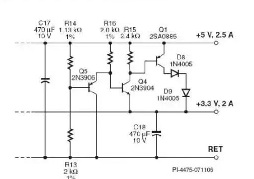
Active Shunt Regulator for Multiple Output Flyback Converters
The circuit works as follows: When both outputs are in regulation, resistor dividers R14 and R13 bias transistor Q5, which in turn keeps Q4 and Q1 off. Under these operating conditions, the current flowing through Q5 acts as a small dummy load at the 5V output.
The standard difference between the 5V output and the 3.3V output is 1.7V. When the load requires additional current from the 3.3V output and the load current from the 5V output does not increase by the same amount, the output voltage will increase compared to the voltage at the 3.3V output. Since the voltage difference exceeds about 100 mV, Q5 will be biased off, turning on Q4 and Q1 and allowing current to flow from the 5V output to the 3.3V output. This current will reduce the voltage at the 5V output, thereby reducing the voltage difference between the two outputs.
The amount of current in Q1 is determined by the difference in voltage across the two outputs. Therefore, the circuit keeps both outputs in regulation regardless of their load, even in the worst case of a full load on the 3.3V output and no load on the 5V output. Q5 and Q4 in the design provide temperature compensation, since the VBE temperature changes in each transistor can cancel each other out. Diodes D8 and D9 are not required but can be used to reduce power dissipation in Q1, eliminating the need to add a heat sink to the design.
The circuit only reacts to the relative difference between the two voltages and is largely ineffective under full and light load conditions. Since the shunt regulator is connected from the 5V output to the 3.3V output, the active dissipation of this circuit can be reduced by 66% compared to a grounded shunt regulator. The result is high efficiency at full load and low power consumption from light to no load.
Four
High-Voltage Input Switching Power Supplies Using StackFETs Industrial equipment that operates on three-phase AC often requires an auxiliary power stage that can provide stable low-voltage DC to analog and digital circuits. Examples of such applications include industrial drives, UPS systems and energy meters.
The specifications for such power supplies are much more stringent than those required by off-the-shelf standard switches. Not only are input voltages higher in these applications, but equipment designed for three-phase applications in industrial environments must tolerate very wide fluctuations—including extended dip times, power surges, and occasional loss of one or more phases. Furthermore, the specified input voltage range of such auxiliary power supplies can be as wide as 57 VAC to 580 VAC.
Designing such a wide-range switching power supply can be a challenge, mainly due to the high cost of high-voltage MOSFETs and the limitations of the dynamic range of traditional PWM control loops. StackFET technology allows the combination of inexpensive, low-voltage MOSFETs rated at 600V and an integrated power controller from Power Integrations to design simple, inexpensive switching power supplies that can operate over a wide input voltage range.
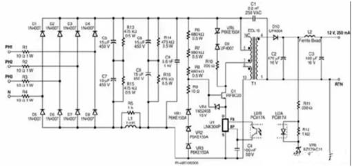
Three-phase input 3W switching power supply with StackFET technology
The circuit works as follows: the input current to the circuit can come from a three-phase three-wire or four-wire system, or even from a single-phase system. The three-phase rectifier consists of diodes D1-D8. Resistors R1-R4 provide inrush current limiting. If fusible resistors are used, these resistors can be safely disconnected during faults without the need for a separate fuse. The pi filter consists of C5, C6, C7, C8 and L1, which can filter the rectified DC voltage.
Resistors R13 and R15 are used to balance the voltage across the input filter capacitors.
When the MOSFET inside the integrated switch (U1) turns on, the source of Q1 will be pulled low, R6, R7, and R8 will provide gate current, and the junction capacitance of VR1 to VR3 will turn on Q1. Zener diode VR4 is used to limit the gate-source voltage applied to Q1. When the MOSFET within U1 is turned off, the maximum drain voltage of U1 is clamped by a 450 V clamping network consisting of VR1, VR2, and VR3. This will limit the drain voltage of U1 to close to 450 V.
Any extra voltage at the end of the winding connected to Q1 is applied to Q1. This design effectively distributes the total rectified input DC voltage and flyback voltage between Q1 and U1. Resistor R9 is used to limit high frequency oscillations during switching, and clamp network VR5, D9 and R10 are used to limit the peak voltage on the primary due to leakage inductance during the flyback interval.
Output rectification is provided by D1. C2 is the output filter. L2 and C3 form a secondary filter to reduce switching ripple at the output.
When the output voltage exceeds the total voltage drop across the optocoupler diode and VR6, VR6 will turn on. Changes in the output voltage cause a change in the current flowing through the optocoupler diode in U2, which in turn changes the current through the transistor in U2B. When this current exceeds the FB pin threshold current of U1, the next cycle is inhibited. Output regulation can be achieved by controlling the number of enable and inhibit cycles. Once the switching cycle is turned on, the cycle ends when the current rises to U1’s internal current limit. R11 is used to limit the current through the optocoupler during transient loads and to adjust the gain of the feedback loop. Resistor R12 is used to bias Zener diode VR6.
IC U1 (LNK 304) has built-in functions and thus protects the circuit against loss of feedback signal, short-circuit at the output, and overload. Since U1 is powered directly from its DRAIN pin, there is no need to add an extra bias winding on the transformer. C4 is used to provide internal power supply decoupling.
five
A good selection of rectifier diodes can simplify and reduce the cost of the EMI filter circuit in the AC/DC converter. This circuit can simplify and reduce the cost of the EMI filter circuit in the AC/DC converter.
To make an AC/DC power supply EMI compliant, a large number of EMI filter components, such as X and Y capacitors, are required. Standard input circuits for AC/DC power supplies all include a bridge rectifier to rectify the input voltage (typically 50-60 Hz). Since this is a low frequency AC input voltage, standard diodes such as 1N400X series diodes can be used, another reason is that these are the cheapest.
These filter devices are used to reduce EMI generated by power supplies in order to comply with published EMI limits. However, since the measurements used to record EMI only start at 150 kHz and the AC line voltage frequency is only 50 or 60 Hz, the reverse recovery time of standard diodes used in bridge rectifiers (see Figure 1) is long, And usually not directly related to EMI generation.
However, input filter circuits in the past sometimes included some capacitors in parallel with the bridge rectifier to suppress any high frequency waveforms caused by the rectification of the low frequency input voltage.
These capacitors are not needed if fast recovery diodes are used in the bridge rectifier. When the voltage between these diodes starts to reverse, they recover very quickly. This reduces stray line inductance excitation in the AC input line by reducing subsequent high frequency turn-off snaps and EMI. Since 2 diodes can be turned on in each half cycle, only 2 of the 4 diodes need to be of the fast recovery type. Likewise, of the two diodes that conduct each half cycle, only one of the diodes needs to have a fast recovery characteristic.

Typical input stage of an SMPS using a bridge rectifier at the AC input

Input voltage and current waveforms show diode snap at the end of reverse recovery
six
Disabling Low-Cost Outputs with Soft-Start to Contain Current Spikes To meet stringent standby power specifications, some multiplex output power supplies are designed to disconnect the outputs when the standby signal is active.
Typically, this is accomplished by turning off a series bypass bipolar transistor (BJT) or MOSFET. For low current outputs, BJTs can be a suitable and less expensive alternative to MOSFETs if the power transformer is designed with the additional voltage drop of the transistors in mind.
Figure 10 shows a simple BJT series bypass switch with a voltage of 12 V, an output current of 100 mA, and a large capacitor (CLOAD). The transistor Q1 is a series pass element, and its switching is controlled by Q2 according to the state of the standby signal. Resistor R1 is rated to ensure that Q1 has sufficient base current to operate in saturation at minimum beta and maximum output current. PI recommends adding an additional capacitor (Cnew) to regulate the transient current at turn-on. If Cnew is not added, Q1 enters the capacitive load quickly after turning on, and thus produces a large current spike. To accommodate this transient spike, the capacity of Q1 needs to be increased, which leads to an increase in cost.
Cnew, used as an additional “Miller capacitor” for Q1, can eliminate current spikes. This extra capacitance limits the dv/dt value of Q1’s collector. The smaller the dv/dt value, the less charging current flows into Cload. Specify a capacitor value for Cnew such that the ideal output dv/dt value of Q1 multiplied by the value of Cnew equals the current flowing into R1.
![]()
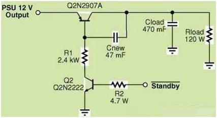
Simple soft-start circuit disables power output during standby while eliminating current spikes during turn-on Therefore, small transistor (Q1) can be used to keep costs low


