Shunlongwei Co. ltd.
IGBT Module / LCD Display Distributor
Customer Service
+86-755-8273 2562
IGBT Module / LCD Display Distributor
When the IGBT is turned off, the operational range of safe operation for VCE-IC is referred to as the Reverse Bias Safe Operation Area (RBSOA). This is also known as the Switching Safe Operation Area, which indicates the maximum allowable transient voltage and current during repeated turn-off operations, as shown in Figure 1. When designing the buffer circuit, it is important to ensure that the VCE-IC trajectory during turn-off remains within this RBSOA region. The RBSOA is divided into two regions: one for typical switching operations (solid line, bidirectional) and the other for high currents (short circuit) (dashed line, non-bidirectional), as denoted in the diagram. For convenience, the area bounded by the solid line is referred to as RBSOA, while the area bounded by the dashed line is referred to as SCSOA (Short Circuit Safe Operation Area). It’s important to note that the SCSOA region tends to narrow as the collector current increases. The IPM includes gate drive and protection circuits that safeguard against operating modes that exceed the IGBT’s safe operating area, thus preventing damage to the module.
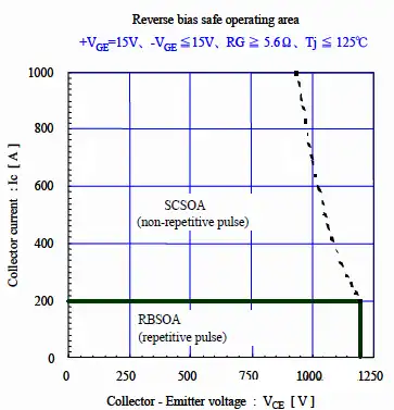
Figure 1: Reverse Bias Safe Operation Area (RBSOA)
Figures 2 and 3 depict the Switching Safe Operation Area and the Short Circuit Safe Operation Area of the IPM/IGBT module.

Figure 2: Switching Safe Operation Area
Operation remains within the safe working area if IOC, VCES, and VCC all stay within their specified values.

Figure 3: Short Circuit Safe Operation Area
Meeting the provided technical specifications generally prevents damage.
Safe Operating Area (SOA) of IGBT/IPM
Short Circuit Safe Operating Area (SCSOA)
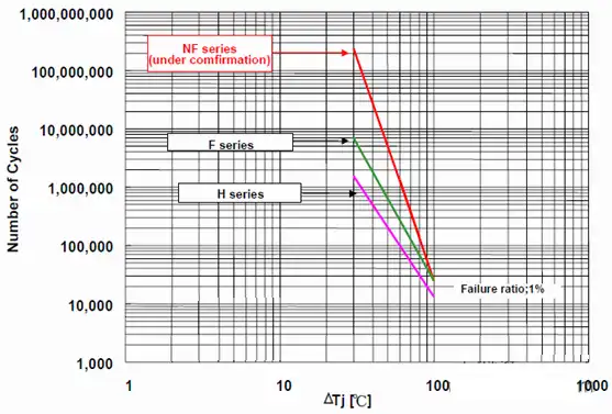
The power cycling lifetime curve of an IGBT module is depicted in the following diagram: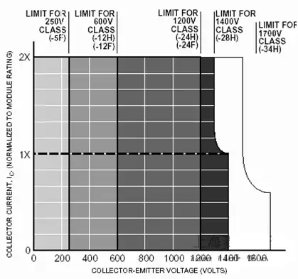
The power cycling lifetime curve of an IGBT module is depicted in the following diagram:
The power cycling lifetime curve of an IPM (using DIP IPM as an example) is shown below:
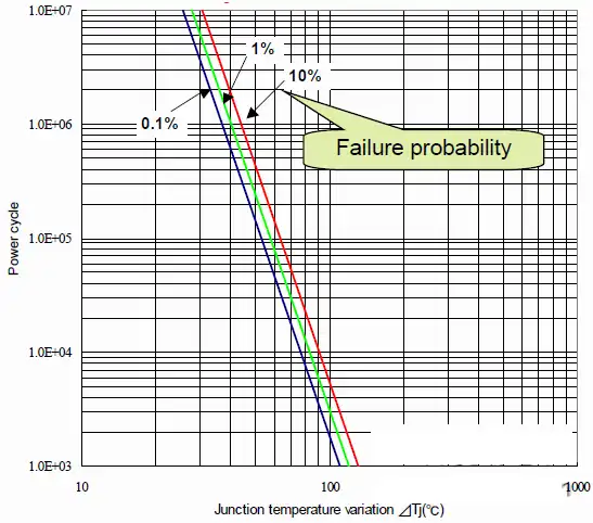
The variation of junction temperature ΔTj in DIP IPM significantly affects power cycling lifetime. To ensure a low failure probability in high-power cycles, it’s essential to avoid drastic changes in device junction temperature.