
Shunlongwei Co. ltd.
IGBT Module / LCD Display Distributor
Customer Service
+86-755-8273 2562
IGBT Module / LCD Display Distributor
“The history of optical communication using light waves as the information carrier has a long history. Atmospheric laser communication uses the atmosphere as the transmission medium, and is the first communication method developed after the emergence of lasers. Because it has the advantages of long transmission distance, wide frequency band, small transmitting antenna, good confidentiality and anti-electromagnetic interference, it has attracted more and more attention, and its application has become more and more widely used.
“
Authors: Huang Haibo, Ai Yong, Liu Lei, Sun Wei
The history of optical communication using light waves as the information carrier has a long history. Atmospheric laser communication uses the atmosphere as the transmission medium, and is the first communication method developed after the emergence of lasers. Because it has the advantages of long transmission distance, wide frequency band, small transmitting antenna, good confidentiality and anti-electromagnetic interference, it has attracted more and more attention, and its application has become more and more widely used.
Ethernet is the most widely used networking technology. It has the advantages of high reliability, large amount of media information, easy expansion and update, etc. It is widely used in enterprises, schools and other fields. According to IEEE802.3 Ethernet standard specification, the length of each coaxial cable of Ethernet shall not exceed 500m, and after interconnection through repeaters, the maximum distance of the network shall not exceed 2.8km. In this case, the use of laser wireless communication technology, beyond the geographical restrictions of Ethernet, to meet the needs of data communication, has a strong application value.
1 Ethernet-based laser wireless communication system
Combining Ethernet and laser wireless communication to give full play to the advantages of both can greatly improve the application range and reliability of the system.
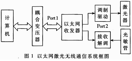
Figure 1 is a schematic block diagram of one end of the Ethernet-based laser wireless communication system, and the structure of the other end is in a symmetrical state with the local end. The bipolar MLT-3 data signal from the computer network card is converted into a unipolar level signal by the RJ45 interface and after passing through the coupling transformer, and sent to the Ethernet transceiver. The generated high-speed PECL signal passes through the modulation drive circuit to the laser Direct intensity modulation drives the laser to emit light, and the information-carrying laser is emitted through an optical antenna. The optical antenna at the receiving end collects the laser signal on the photosensitive tube. After passing through the receiving and demodulating circuit, the PECL high-speed data signal is recovered, and then sent to the computer through the coupling transformer to complete the entire communication process. It can be seen from Figure 1 that the system is mainly composed of three parts: Ethernet transceiver, modulation driving circuit and receiving demodulation circuit. The circuit design of these three parts is described in detail below.
2 Ethernet transceiver circuit
The Ethernet transceiver circuit is composed of RJ45 interface, coupling transformer, Ethernet transceiver, and the interface between the transceiver, modulation driving circuit, and receiving demodulation circuit. The Ethernet transceiver is the core unit, which directly determines the performance of the system.
2.1 Ethernet transceiver IP113
The system uses the Ethernet to fiber transceiver IP113 chip produced by IC PLUS. IP113 is a two-port (including TP port and FX port) 10/100Mbps Ethernet integrated switch, consisting of a two-port switch controller and two Ethernet fast transceivers. Each transceiver complies with IEEE802.3, IEEE802.3μ, IEEE802.3x rules. The SSRAM is reserved for the frame buffer, which can store 1K bytes of MAC address, all-digital adaptive adjustment and timing recovery, baseline drift correction, and works in full-duplex/half-duplex mode of 10/100baseTX and 100baseFX. Use 2.5V single power supply, 25MHz single clock source, 0.25μm process, 128-pin PQFP package.
Figure 2 is a block diagram of the internal principle of IP113. IP113 works in store-and-forward mode, and the rate of Port1 (TP port) is the result of adaptive adjustment, so no additional memory is needed to buffer data packets. Each port has its own receive buffer management, transmit buffer management, transmit queue management, transmit MAC and receive MAC. Each port shares a hash unit, a memory interface unit, an empty buffer manager, and an address table. The hash unit is responsible for finding and identifying addresses. Transmit buffer management and receive buffer management are responsible for storing or reading data through the memory interface. The transmitting MAC and the receiving MAC are responsible for completing various protocol controls of the Ethernet. After the receiving MAC receives the data from the transceiver, it is put into the receiving FIFO, and at the same time requests the receiving buffer management for the data transmission. When the receiving buffer management receives the request, it obtains an empty storage block from the empty buffer management area, and writes the data packet through the memory interface unit. At the same time received packets also enter the hash unit. The hash unit finds the address from the packet to build the address table. IP113 decides whether to forward or discard the data packet according to the address table. Both ports share an empty buffer management, which provides empty memory areas for both addresses after reset. When a data packet is received, a new empty storage area is found; when a data packet is forwarded, the corresponding storage area is released.

2.2 Ethernet transceiver circuit design
The Ethernet transceiver circuit is shown in Figure 3. It is mainly composed of Ethernet transceiver chip IP113, special configuration chip EEPROM 93C46, LED Display matrix, and the interface between Port1 and TP module, Port2 and FX module of IP113.
IP113 supports many functions, which can meet different needs by setting appropriate parameters, which can be set by specific pins or configured by EEPROM. In order to improve the overall performance of the system, a dedicated serial EEPROM 93C46 chip is used here. When the system is reset, pins LED_SEL[1:0]are used as 93C46 clock EESK and chip select EECS respectively, BP_KIND[1:0]are used as 93C46 address EEDI and data output EEDO respectively, and the internal parameters of 93C46 are read into the internal registers of IP113 . After reset, these pins become input signals, so that IP113 can work independently from 93C46.
When reset, IP113 first reads the content in 00H of 93C46, only when 00H[15:0]=55AAH, will it continue to read parameters from EEPROM, otherwise it will work with default value or specific pin level value setting register. The value in 01H sets the LED output control register to control the on, off and flashing of the two LED matrices to display the connection, activity, full/half duplex and speed (10Mbps/100Mbps) of the two ports, respectively. The value in 02H sets the exchange control register 1, and selects the flow control mode and conflict protection of the system. The value in 03H sets the switch control register 2, which controls the system’s packet loss, address invalidation, priority and algorithm compensation. The value in 04H sets the transceiver control register, of which the five values of 04H[13:11]are: 000, 100, 101, 110 and 111, which correspond to the five working states of the transceiver: NWAY, 10Mbps (half-duplex). ), 10Mbps (full, half duplex), 100Mbps (half duplex), and 100Mbps (full, half duplex). The values in 05H~0AH set the transceiver confirmation register, test register and verification mode register respectively.
TXOP and TXOM of Port1 are TP transmit data pairs, RXIP and RXIM are TP receive data pairs. In the TP module circuit in Figure 4, the RJ45 interface converts the MLT-3 code stream Ethernet signal into a unipolar signal through the coupling pulse transformer PE68515.
Port2’s FXRDP and FXRDM are FX’s receiving data pair, and FXTDP and FXTDM are FX’s transmitting data pair. FXSD is a photoelectric detection signal. When the received optical signal is photoelectrically converted and the level is lower than 1.2V, the FXSD outputs a continuous PECL level. Figure 5 is the circuit diagram of the FX module, and the standard FDDI data interface is used in the circuit. Since the modulation driving and receiving demodulation circuits use 5V power supply, and other parts of the system use 2.5V power supply, the signals in the FDDI are all PECL level, so they must be level-shifted (as shown in Figure 5), in order to convert this Connect the two parts.
3 Modulation drive circuit design
Fig. 6 is the modulation driving circuit diagram, which is mainly composed of the MAX3263 chip of 155MHz of MAXIM Company and the laser LD with monitor diode inside. The main bias power supply inside MAX3263 provides temperature-compensated bias and reference voltage outputs Vref1 and Vref2, through resistors R25, R26, R27 and R28 to program the internal high-speed modulation drive circuit, laser and monitor diode. The output current of the MAX3263 is controlled by the internal mirror current sources. These mirror current sources have a junction temperature drift of 2Vbe. When the reference voltage is set at 2Vbe, the junction temperature drift can be offset. Resistor R28 is selected to adjust the static bias current Ibo of the laser, so that Ibo is slightly smaller than the threshold current of the laser, so that the output of the laser has a good extinction ratio. The monitoring diode inside the LD converts the light intensity change into a current Ipin, and the feedback current Ibs is generated by the internal conversion. By the formula Ibo=40 (Ib+Ibs), the light intensity change of the laser is converted into a part of the bias current, and the feedback acts on the laser. To ensure stable output optical power. The input differential PECL signals RD and RD are modulated by a modulator composed of an internal high-speed input buffer and a common emitter differential output, and the size of the modulating current is determined by the current Im determined by R26. The size of R26 is selected so that the laser has an appropriate modulation current, outputs sufficient optical power, and has a good extinction ratio. At the same time, the voltage of the OUT+ and OUT- terminals should be above 2.2V to prevent the laser from being saturated.
4 Receive and demodulate circuit design
Fig. 7 is the circuit diagram of receiving demodulation, which is composed of MAX3963 and MAX3964 with necessary peripheral devices. The 155MHz low-noise chip MAX3963 constitutes a preamplifier, which contains a transimpedance preamplifier and an inverting amplifier with an emitter follower output, and integrates a 22kΩ transimpedance, which can convert the weak photocurrent received by the PIN into Differential output voltage. The MAX3964 of 266MHz forms the post-stage amplifying and conditioning circuit. It has a serial power detector composed of four limiting amplifiers, and each limiting amplifier has a full-wave logarithmic detector to detect the power of the input signal. The four detection results are added together at the Filter end, and filtered through the capacitor C25. Resistors R30, R31, the internal 1.2V reference power supply and the non-light comparator together constitute the threshold setting and noise suppression functions. Take R30 = 100kΩ, R31 can be adjusted with a 100kΩ potentiometer, then VTR changes between 1.2 and 2.4V. When the input signal amplitude is greater than VTR, output a stable PECL level signal; when the input signal amplitude is less than VTR, the data output terminal OUT+ outputs a high level, OUT- outputs a low level, and all limiting amplifiers refuse to receive the input signal, and the post-stage amplifier outputs the no-light alarm PECL signal LOS+.
Since the main chips in Fig. 6 and Fig. 7 are all above 155MHz, the transceiver circuit is composed of these two circuits, which can be applied to high-speed optical communication occasions through careful parameter selection and PCB design.
5 System Test
On the basis of the designed parts, they are connected together, and the experiment of indoor Ethernet laser wireless communication is successfully carried out without optical antenna. The system is being perfected and ready to be applied to optical networks.
The Links: SCE200AA160 A50L-0001-0331

