
Shunlongwei Co. ltd.
IGBT Module / LCD Display Distributor
Customer Service
+86-755-8273 2562
IGBT Module / LCD Display Distributor

Called STGAP2GS the wide body SO-8W packaged single-channel driver can work with rails up to 1.2kV, or 1.7kV for the STGAP2GSN narrow body SO-8 version, said ST.
According to the data sheets, the the lower-voltage-rated ‘wide’ package is 5.8mm long by 10.3mm across pins tips, with 7.5mm between pin roots – where the isolation voltage would be required, and the higher-voltage-rated narrow package is 4.9mm long by 6mm across pin tips, with only 3.1mm between pin roots. electronics Weekly has asked what allows the narrower-packaged device to have a higher voltage rating.

A separate supply (above), or dual supplies (left) if a negative off-voltage is required at the gate, is required on the output side. This can be at up to 15V.
Output capacity of 2A source and 3A sink, and there are separate source and sink outputs to allow different series resistors to be added to independently optimise turn-on and turn-off.
The input-side supply can be 5V or 3.3V, and the signal input has hysteresis for snappy switching.
High-to-low and low-to-high transistion delays are matched through the device. Maximum propagation delay input to output is 70ns across the -40 to +125°C operating junction temperature range with a 5V input supply, and 90ns at 3.3V. Typical 25C figures are 42ns at 5V and 55ns at 3.3V.
Output rise and fall times are 30ns with a 4.7nF load.
“Transient immunity of ±100V/ns over the full temperature range guards against unwanted transistor gate change,” said ST. “The driver features built-in system protection including thermal shut-down and under-voltage lock-out optimised for GaN technology.”

On top of this, internal circuits keep the output drivers in a safe state (keeping the external device off) until all voltages are properly established, and a watchdog turns off the external device if communication across the isolation barrier is lost.
There are two inputs, allowing either polarity of PWM to be applied.
These include adjustable dead-time generation for the half-bridge output stage, and so accept a simple PWM input.
On-board isolated (5.2kV) dc-dc converters provide the secondary side with power, and gate drive can be set at +6V/0V or +6V/-3V.
Consumer and industrial applications are foreseen, including in servers, factory-automation, motor drivers, solar power, wind power, home appliances and wireless chargers.
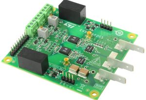
Find the STGAP2GS web page here and its evaluation board here – or the narrow STGAP2GSN here and its eval board here


