
Content last revised on September 15, 2026
Assembly Integrity & Layout Architecture: Implementing Active Miller Clamp for MIG50J901H
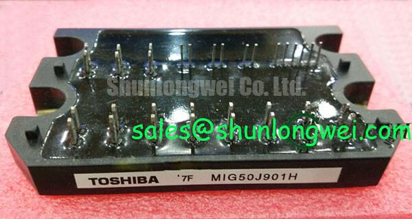
Before connecting the gate drive, verify the equipment nameplate against the module rating and inspect the terminal area, baseplate, and insulation surfaces for damage, contamination, or mounting marks that could affect installation. The MIG50J901H is a Toshiba three phase inverter IGBT module rated at 600 V collector emitter voltage and 50 A collector current. These are Official Datasheet Specifications and define the electrical boundary that must be checked against the original drive design before a repair or replacement decision.
| Official parameter | Specification |
|---|---|
| Manufacturer | Toshiba |
| Collector Emitter Voltage VCES | 600 V |
| Collector Current IC | 50 A |
| Collector Power Dissipation PC | 150 W per element |
| Isolation Voltage VISOL | 2500 V AC for 1 minute |
| Topology | Three Phase Inverter |
| Protection Functions | OC, UV, OT, Fault Output |
For a heavy duty variable frequency AC motor drive, the three phase inverter topology should be evaluated as part of the existing power stage rather than as an isolated switching part. Confirm the original terminal assignment, driver board connection, DC link polarity, phase output routing, cooling arrangement, and control supply sequence from the equipment documentation. The listed OC, UV, OT, and fault output functions identify available protection functions, but their exact response thresholds, timing, and external wiring requirements must be verified from the original system documentation.
Active Miller clamping is a Design Consideration when a gate driver must prevent an inactive IGBT from being disturbed by rapid collector voltage movement. During switching, current through parasitic capacitances can raise the gate potential of the nominally off device. If the gate return path has excessive inductance or shares a noisy power return, this disturbance can contribute to unintended conduction. A dedicated low impedance clamp path placed close to the driver and gate return can reduce that risk, subject to validation with the actual driver, wiring, and switching conditions.
Negative gate turn off bias is also a Design Consideration, not an official operating voltage specification for this module. Where the existing drive architecture uses a negative off state bias, the system integrator should confirm that the gate driver, isolation arrangement, gate resistor network, and device operating limits support it. Do not transfer gate drive settings from another inverter module without checking the original design documentation and measured switching waveform behavior.
Keep the gate loop physically separate from high current collector and emitter paths wherever the assembly permits. Route the driver output and its return as a closely coupled pair, avoid long common return sections, and place gate related connections so that phase current does not flow through the control reference. These measures are Engineering Recommendations intended to reduce common mode ground movement and false gate triggering. They do not replace a switched waveform measurement at the installed operating condition.
Practical warning: Isolate and verify the DC link has discharged before unplugging a driver connector, because stored energy and an uncontrolled gate state can damage the inverter stage.
When a repair involves a driver board change, inspect the complementary gate commands at the module connection with suitable isolated measurement equipment. A missing command, asymmetric transition, or a fault output that does not match the controller state may indicate an issue in the driver path, interlock logic, supply reference, or measurement arrangement. Compare against a known good channel or validated service information instead of assigning a single cause from one waveform.
Transient Dynamics & Electrical Design: DC Link Capacitance Bank Layout and Low ES on MIG50J901H
The 600 V VCES rating must be treated as an Official Datasheet Specification, while the actual transient voltage at the MIG50J901H terminals is determined by the surrounding inverter assembly. At turn off, peak voltage is governed by the DC link voltage together with the inductive contribution associated with changing current. In practical terms, reducing the commutation loop inductance reduces the overshoot that must be accommodated during switching. The system engineer should verify peak collector emitter voltage on the installed drive during representative switching tests.
DC link capacitors should be positioned and connected to provide a short, low inductance commutation path to the inverter module. A compact symmetric laminated or planar busbar arrangement is commonly evaluated as a Design Consideration because it can reduce loop area and promote similar electrical conditions across phase legs. The suitability of a specific capacitor bank, busbar geometry, snubber network, and connection hardware remains system determined. It should be verified against measured switching current, DC link conditions, cable routing, and thermal loading.
A snubber capacitor or other transient control network should only be selected after the existing drive topology and measured ringing characteristics are understood. Added capacitance can alter switching energy, resonant behavior, and fault response. A repair engineer should first inspect for loose DC link connections, displaced busbars, degraded capacitor terminations, damaged suppression components, or an altered physical current path. These conditions can affect overshoot and electromagnetic noise without changing the MIG50J901H itself.
Complementary gate interlock and dead time are system level functions that prevent the upper and lower devices in a phase leg from being commanded on simultaneously. The necessary timing depends on the driver propagation behavior, switching conditions, load current, temperature, and observed gate waveforms. An Engineering Recommendation is to preserve the original controller timing during an equipment repair unless it is being revalidated through controlled testing. Changes made solely to correct a visible current imbalance can conceal an underlying driver or layout problem.
Long motor cables are another system condition worth checking in a variable frequency AC motor drive. Cable impedance and propagation effects can produce voltage reflections at the motor terminals, and the resulting stress is not defined by the module rating alone. The existing output filter, motor insulation class, cable length, grounding arrangement, and switching strategy should be reviewed together. Where waveform control is necessary, validate the drive output with appropriate measurement methods rather than assuming a module replacement resolves cable related voltage behavior.
For a broader technical discussion of switching loss, drive conditions, and measured margin assessment, maintenance teams can consult Unlocking Efficiency in Industrial Drives as supporting engineering reference material. General awareness of conducted and radiated switching noise can also be supported by the external reference on electromagnetic interference. This reference does not establish EMC compliance for the MIG50J901H or for any completed drive.
Transient Dynamics & Electrical Design: Multi Module Parallel Current Sharing on MIG50J901H
Parallel operation should not be assumed from the 50 A collector current rating alone. The MIG50J901H is specified as a three phase inverter module, and any arrangement involving multiple modules requires a complete review of circuit topology, current return paths, thermal interfaces, driver timing, protection coordination, and fault clearing behavior. The 150 W per element dissipation value is an Official Datasheet Specification, not a statement that equal thermal or electrical sharing will occur in a particular parallel assembly.
At steady state, the temperature behavior of IGBT saturation voltage can contribute to current sharing under appropriate operating conditions. That tendency is a Design Consideration, not a guarantee of acceptable balance. Dynamic sharing is often more sensitive to unequal gate loop inductance, resistor placement, driver output impedance, DC link geometry, and phase current path length. A physically symmetric layout helps reduce these differences, but only measurement under the intended load and switching conditions can establish whether current division is acceptable.
When evaluating a drive with two inverter modules, compare the physical orientation of each module, busbar length, capacitor connection location, gate harness routing, heat sink contact pattern, and control reference return. Do not use a single gate resistor location or a shared gate return that creates different loop behavior between parallel devices. Designers should verify current waveforms and gate voltage behavior for each participating path with measurement methods appropriate to the voltage and energy present in the equipment.
Protection coordination deserves the same attention as current balance. The MIG50J901H lists OC, UV, OT, and fault output protection functions, yet parallel operation may require the host controller to interpret protection indications from more than one location. The repair team should confirm how the original equipment manages a detected fault, including whether all related gate commands are removed and whether the control system records a diagnostic condition. Do not infer protection timing, short circuit capability, soft shutdown behavior, or safe operating duration from the parameter list provided here.
A related Toshiba inverter module, MG100Q1ZS40, can be examined as a separate reference point during a documented compatibility assessment. It should not be treated as a direct substitute on the basis of current rating or package appearance. Terminal mapping, voltage class, protection interface, driver compatibility, mechanical fit, cooling requirements, and measured switching behavior must all be verified by the responsible system engineer.
In a complete drive power chain, an associated module such as MG150Q1JS40 may appear in a different conversion or power stage depending on the equipment architecture. Its presence does not establish interchangeability with the MIG50J901H. Record each installed module's functional position before commissioning so that rectification, inverter switching, braking, and auxiliary power functions are not conflated during troubleshooting.
Assembly Integrity & Layout Architecture: Implementing Thermal Interface Material Thickness Uniformity for MIG50J901H
Before final tightening, clean the mating surfaces and inspect the MIG50J901H baseplate and heat sink for flatness concerns, embedded debris, scratches, corrosion, or old interface compound that could prevent uniform contact. The module's 2500 V AC isolation voltage for 1 minute is an Official Datasheet Specification for its stated test condition. It is not a substitute for verifying the insulation system, creepage paths, mounting arrangement, enclosure, or service safety requirements of the complete motor drive.
Thermal interface material should be applied as a controlled, continuous layer that fills surface irregularities without creating excessive thickness or trapped voids. Thickness uniformity is a Design Consideration because the appropriate material, application method, and final bond line depend on the actual baseplate condition, heat sink finish, interface compound properties, and clamp arrangement. Excess material can increase thermal resistance, while incomplete coverage can create localized hot areas. Visual inspection of the contact transfer pattern after a controlled trial installation can help identify an uneven interface.
Use a sequential fastening pattern that brings the module down evenly across the heat sink surface. The torque value, screw type, washer arrangement, and tightening order should come from the module documentation and the equipment mechanical design. If spring washers or other force control hardware are part of the original assembly, preserve their orientation and placement unless a qualified mechanical review defines a change. Uneven mounting force can distort the contact plane, alter thermal behavior, and place unnecessary stress on terminals or insulating hardware.
For equipment using a clamped power assembly rather than a conventional baseplate fastener arrangement, force calibration must be treated as a system mechanical requirement. The applicable pressure, spring stack configuration, electrical insulation components, and double sided cooling arrangement must be verified from the original assembly documentation. Do not adapt baseplate mounting practices to a pressure contact construction without an approved mechanical design, because the electrical and thermal interfaces are fundamentally different.
After reassembly, inspect the phase terminals and DC connections for correct seating, consistent mechanical support, and clearance from adjacent conductive parts. Then evaluate cooling airflow, fan operation, heat sink cleanliness, temperature sensing path, and controller fault response before applying full load. If an overtemperature indication occurs, it may relate to thermal interface condition, cooling performance, sensor circuit behavior, load profile, or protection logic. A controlled test sequence and comparison with validated equipment information provide a more reliable basis for diagnosis than a single temperature reading.
