
Industrial TFT-LCD LVDS Timing, Backlight Driver Matching, and HMI Field Replacement Engineering
Replacing an industrial TFT-LCD module inside a CNC controller, PLC operator station, or medical monitor appears mechanically straightforward when diagonal size and resolution match. In practice, field technicians frequently encounter distorted colors, rolling frames, blank screens after boot, or premature backlight shutdown. These failures rarely stem from defective glass; they commonly trace back to mismatches in LVDS differential timing, 6-bit versus 8-bit color mapping (JEIDA vs. VESA), power-up sequencing, or backlight driver electrical compliance.
This engineering guide breaks down the physical signaling and power-delivery boundaries governing industrial display integration, giving maintenance and design engineers a deterministic framework for drop-in replacement and retrofit qualification.
1. What Governs Industrial TFT-LCD Signal Integrity and Display Stability?
An industrial TFT-LCD panel is not a passive monitor; its internal timing controller (T-CON) acts as a strict state machine that expects synchronized pixel clocks, valid blanking intervals, and deterministic logic-rail rise times. Unlike consumer HDMI or DisplayPort monitors that negotiate capabilities dynamically over an AUX/DDC channel via EDID, most industrial panel-level interfaces use LVDS (Low-Voltage Differential Signaling) as the physical signaling layer, often implemented via serialized display interface architectures such as Texas Instruments’ FPD-Link.
Because LVDS is unidirectional from the host single-board computer (SBC) or graphics controller to the panel T-CON, the display cannot automatically correct mismatched clock frequencies, inverted Data Enable (DE) polarities, or misaligned color bit slots. Understanding the underlying electrical and protocol boundaries prevents costly commissioning delays during equipment downtime.
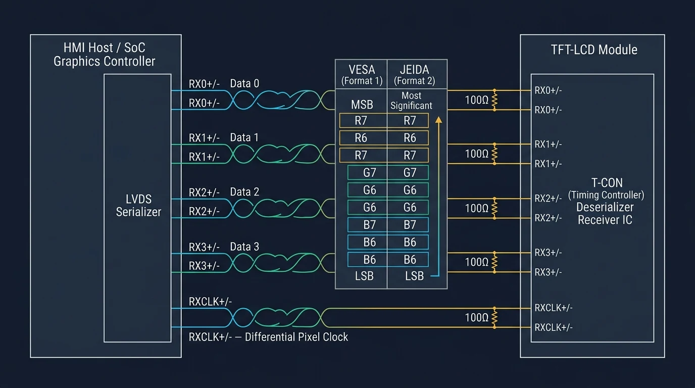
2. LVDS Physical Layer, Differential Termination, and EMI Boundaries
At the physical layer, LVDS transmits serialized pixel data and clock signals over tightly coupled differential wire pairs. According to the Texas Instruments LVDS Owner’s Manual, standard LVDS operates with a nominal differential output voltage (VOD) around 350 mV centered on a common-mode offset (VOC) near 1.2 V. A 100-ohm differential termination resistor—integrated inside the T-CON receiver or placed externally near the receiver inputs—converts the current-loop drive back into a clean differential voltage swing while suppressing reflections.
When retrofitting or replacing a display harness inside high-EMI cabinets (such as VFD-driven machine tools), several physical constraints govern signal margin:
- Differential Pair Impedance and Skew: LVDS harnesses should maintain a controlled 100-ohm differential impedance. Mixing twisted and untwisted ribbon conductors or routing LVDS harnesses parallel to AC motor leads introduces common-mode noise and intra-pair skew, manifesting as sparkling pixels or intermittent horizontal tearing.
- Single-Channel vs. Dual-Channel Partitioning: Whether a panel uses single-channel LVDS (3 data pairs + 1 clock pair for 6-bit, or 4 data pairs + 1 clock pair for 8-bit) or dual-channel LVDS (odd/even pixel splitting across 8 data pairs + 2 clock pairs) depends on pixel clock rate, color depth, transceiver bandwidth, and the specific panel design rather than resolution or diagonal size alone. For example, many XGA/WXGA modules operate over a single channel, whereas higher-bandwidth 1080p industrial displays such as the 21.5-inch G215HAN01.1 commonly adopt dual-channel LVDS to keep per-lane bit rates within transceiver limits.
- Pin-1 Orientation and Connector Pitch Traps: Industrial panels commonly use 20-pin or 30-pin Hirose DF14/DF19 or I-PEX Cabline connectors. Even when two panels share a 20-pin 1.25 mm pitch header, VCC and GND pin assignments can differ between manufacturers—applying 3.3 V or 5 V across an LVDS receiver pair permanently damages the T-CON input stage.
fDCLK = (Hactive + Hblank) × (Vactive + Vblank) × frefresh
As shown in the pixel-clock relation above, the required LVDS clock frequency depends not only on active resolution (Hactive × Vactive), but also on horizontal and vertical blanking intervals (front porch, sync pulse width, and back porch). For example, an XGA panel running at 60 Hz with standard VESA blanking operates near 65 MHz, whereas a VGA 8.4-inch HMI panel such as the AA084XA03 or SVGA 10.4-inch panel like the AA104VJ02 runs at substantially lower pixel clocks—making clock-range verification against the panel datasheet mandatory before substitution.
3. JEIDA vs. VESA Bit Mapping and 6-Bit/8-Bit Color Inversion
One of the most frequent field replacement symptoms is an image that renders cleanly in shape and text, yet displays washed-out highlights, solarized gradients, or inverted primary colors. This almost never indicates a broken LCD; it is a classic LVDS data-mapping mismatch between VESA/NS and JEIDA formats (with VESA/NS mapping commonly referenced in SPWG panel specifications).
In an 8-bit LVDS link (4 data pairs + 1 clock pair), 24 bits of RGB color plus HSYNC, VSYNC, and DE occupy 28 bit slots per clock cycle across four lanes (RX0 through RX3). The difference lies in where the Most Significant Bits (MSBs: R7, R6, G7, G6, B7, B6) and Least Significant Bits (LSBs: R1, R0, G1, G0, B1, B0) are placed:
| LVDS Mapping Attribute | VESA / NS Format | JEIDA Format | Field Mismatch Symptom |
|---|---|---|---|
| MSB Placement (R7/R6, G7/G6, B7/B6) | Mapped onto Pair RX3 | Mapped onto Pairs RX0–RX2 | Solarized skin tones, metallic/neon gradients |
| LSB Placement (R1/R0, G1/G0, B1/B0) | Mapped onto Pairs RX0–RX2 | Mapped onto Pair RX3 | Dark banding or crushed shadows |
| 6-Bit Receiver Compatibility | Requires 6-bit truncation or bit mapping (implemented at the transmitter or receiver depending on interface design) when driven by an 8-bit host | Potentially compatible when RX3 is omitted, provided host bit packing matches receiver 6-bit mapping | Severe contrast distortion if 8-bit VESA drives 6-bit panel |
| Hardware Selection Pin | Typically SEL68 / MAP pulled LOW or HIGH (check datasheet) |
Opposite logic level on SEL68 / MAP pin |
Corrected cleanly via harness strap or BIOS LVDS option |
As detailed in the TI FPD-Link LVDS Display Interface Application Note, JEIDA places the six MSBs of each color channel on the first three data lanes (RX0–RX2) and relegates the two LSBs to the fourth lane (RX3). Consequently, an 8-bit JEIDA transmitter can often drive a 6-bit panel by leaving RX3 unconnected, provided the host serializer’s bit packing and the panel T-CON’s expected 6-bit lane mapping align. By contrast, VESA places the two MSBs on RX3; if an 8-bit VESA host drives a 6-bit panel or a panel strapped for JEIDA, the panel mistakes mid-order bits for the MSBs, causing immediate solarization. Many industrial panels provide a dedicated MAP or SEL68 configuration pin on the LVDS connector—verifying its required logic state (3.3 V vs. GND) resolves color inversion without modifying host firmware.
4. Timing Modes (DE-Only vs. HV Sync) and Power-On Sequencing
Beyond pixel mapping, industrial T-CONs enforce strict synchronization modes and power-rail sequencing:
- DE-Only Mode vs. HV Sync Mode: Modern industrial TFT modules predominantly operate in DE-Only (Data Enable) mode, ignoring discrete HSYNC/VSYNC pulses and relying solely on the active-high DE envelope to frame each horizontal line and vertical frame. Older controllers configured for fixed HV Sync pulses without an active DE signal will produce a black screen or a locked white raster when paired with a DE-only panel.
- Frame Buffer and Porch Tolerance: Some legacy PLC graphics cards output non-standard blanking periods. If Hblank or Vblank falls below the T-CON’s minimum porch window, the image shifts horizontally or exhibits vertical roll.
- Power-On / Power-Off Sequence: To prevent latch-up in source/gate driver ICs and avoid residual DC charge accumulation across the liquid crystal cell (which causes image sticking), panel datasheets specify strict power-on and power-off timing windows: in typical designs, VCC logic power stabilizes before LVDS data/clock signals begin toggling, and LVDS signals stabilize before backlight enable (BL_EN) is asserted, with reverse ordering on shutdown. Always follow the exact inter-rail delay limits specified in the target panel datasheet, as required timing tolerances vary by T-CON architecture.
5. Backlight Architecture: CCFL Inverter Diagnostics vs. Constant-Current LED Retrofits
A significant number of apparent “dead screen” field calls in legacy industrial machinery stem from backlight subsystem failures rather than damaged TFT glass. Understanding the electrical boundary between legacy Cold Cathode Fluorescent Lamp (CCFL) assemblies and modern LED backlight modules is essential before ordering a replacement panel or retrofit kit.
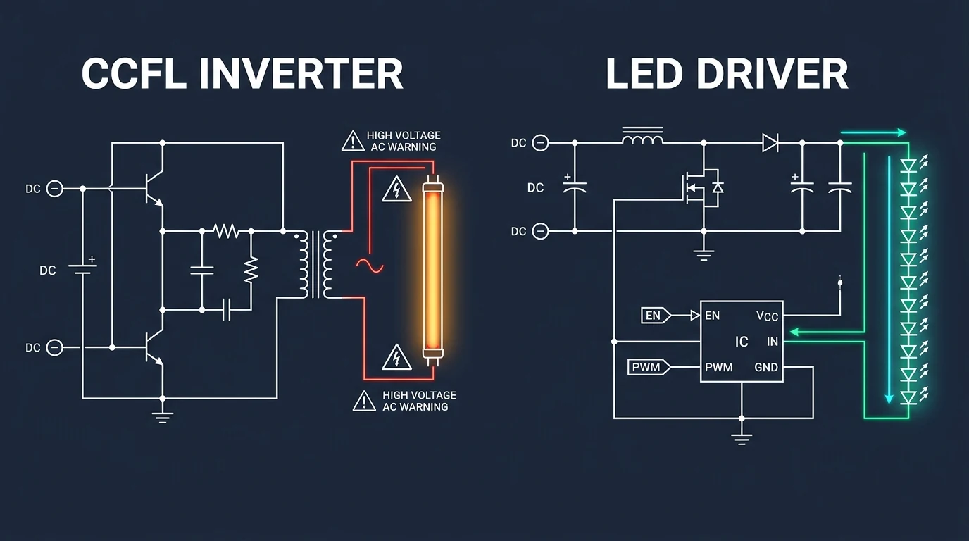
CCFL Backlight Constraints
Older industrial displays—including classic 12.1-inch and 15.0-inch workhorses such as the LQ121S1LG44 and LM151X05-B3 (depending on exact revision suffix)—originally relied on single or dual CCFL tubes driven by an external DC-to-AC inverter board. CCFL tubes require an elevated high-voltage ignition (striking) pulse—commonly in the 600 Vrms to 1,500 Vrms reference range at cold startup—before transitioning to a lower steady-state sustaining voltage at high frequency (typically tens of kilohertz), with exact strike and operating values dictated by the specific lamp length and inverter datasheet. Aged CCFL lamps commonly exhibit pink/reddish tint during warm-up, an increased striking-voltage requirement, and eventual inverter over-voltage or open-lamp protection shutdown shortly after startup.
Constant-Current LED Driver Matching
Modern industrial panels use series-parallel strings of high-efficacy white LEDs driven by a constant-current (CC) boost or buck-boost regulator. When migrating from a CCFL panel to an LED-backlit equivalent—or installing an LED backlight conversion strip—engineers must verify three electrical parameters rather than relying on voltage alone:
- Forward Voltage (VF) Compliance Window: An LED driver regulates current (IF), not voltage. The driver’s boost stage must have an output compliance range that covers the panel’s total string forward voltage across illustrative industrial design conditions—such as cold-start (-20 °C to -30 °C, where VF rises) and elevated ambient (+70 °C)—while verifying actual operating limits against the specific panel and LED driver datasheets.
- Integrated vs. External LED Driver: Some industrial panels integrate the LED constant-current driver directly onto the rear PCB (requiring only 12 V DC,
BL_EN, andPWMon a 6-pin header), whereas others expose raw LED anode/cathode strings that require an external constant-current driver board. - PWM Dimming Frequency and Polarity: Backlight dimming typically accepts either an analog DC voltage (0–3.3 V / 0–5 V) or a PWM logic signal (commonly 100 Hz to 20 kHz, depending on the driver IC). Mismatched active-high vs. active-low
BL_ENor inverted PWM duty cycle causes the panel to boot at 0% brightness or invert the operator’s HMI brightness slider.
6. Field Replacement & Retrofit Verification Checklist
Before powering up a replacement TFT-LCD module in a production cabinet, execute the following deterministic bench-verification sequence:
| Verification Stage | Key Parameter to Confirm | Prevented Failure Mode |
|---|---|---|
| 1. Logic Power (VCC) | Verify 3.3 V vs. 5.0 V rail on host SBC & pinout match | Instant T-CON ESD/latch-up damage |
| 2. LVDS Topology | 1-ch vs. 2-ch, 6-bit vs. 8-bit, pixel clock within fDCLK min/max | Half-screen image, rolling sync, no-display |
| 3. Bit Mapping | Confirm JEIDA vs. VESA strap on MAP / SEL68 pin |
Solarized gradients & inverted primary colors |
| 4. Backlight Loop | CCFL HV inverter vs. CC LED driver; check VF & PWM polarity | 1-second shutdown, dark screen, burned LED strip |
| 5. Mechanical & Thermal | Active area centering, bezel gasket clearance, chassis airflow | Mura pressure spots & high-temp polarizer yellowing |
Maintaining strict alignment across LVDS signal integrity, color mapping, and backlight current regulation turns emergency HMI replacement from trial-and-error troubleshooting into a predictable, repeatable engineering procedure. For broader panel selection principles, optical bonding trade-offs, and environmental derating guidelines, refer back to our Ultimate Guide to Industrial TFT LCD Technology.