
In high-power industrial inverters, traction motor drives, and grid-tied energy storage systems, Insulated Gate Bipolar Transistors (IGBTs) are subjected to extreme electrical stress during hard turn-off transitions. To minimize turn-off switching loss (Eoff), gate drivers are engineered to rapidly discharge the input capacitance, driving collector current down at steep slopes (di/dt often exceeding 2,000 to 5,000 A/μs). However, every real-world busbar geometry, module package, and DC-link connection carries unavoidable parasitic stray inductance (Lstray). When high di/dt collides with Lstray, the magnetic energy stored in the commutation loop induces severe transient voltage overshoot across the collector-emitter terminals:
VCE(peak) = VDC + Lstray × (-di/dt)
If this dynamic overvoltage exceeds the silicon blocking capability (VCES), destructive breakdown can occur, depending on the peak voltage, avalanche current density, pulse duration, and intrinsic device ruggedness. Power electronics design engineers have traditionally relied on two competing philosophies to mitigate this risk: passive snubber networks and active clamping. While both approaches constrain peak terminal voltage, their underlying physical energy-dissipation mechanisms, thermal penalties, and component counts diverge fundamentally.
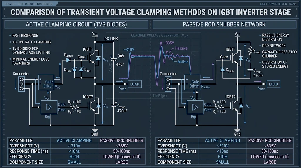
1. The Physics of Turn-Off Transients: Why Stray Inductance Demands Overvoltage Clamping
In a standard half-bridge power stage, the turn-off commutation loop consists of the upper and lower IGBT modules, the laminated DC busbars, and the DC-link decoupling film capacitors. In illustrative high-power industrial benchmarks (for example, switching 400 A to 800 A under an optimized planar laminated busbar geometry with sub-20 nH stray inductance and nominal di/dt of 2,000 to 5,000 A/μs), turn-off transitions induce baseline inductive overshoots in the range of 40 V to 100 V; however, during severe load-dump or fault-clearing conditions with steeper di/dt or in less optimized layouts with higher parasitic inductance, transient spikes can surge several hundred volts above the continuous DC bus voltage (VDC).
Consider a continuous DC-bus voltage of 800 V paired with a standard 1200 V IGBT module, such as the widely deployed SKM100GB12T4 (1200 V / 100 A) or the heavy-duty FF450R12ME4 (1200 V / 450 A). When evaluating an illustrative engineering derating target of approximately 80% of VCES (e.g., a 960 V operating threshold for a 1200 V device), only ~160 V of dynamic voltage headroom remains under full operating bias. Any sudden load-dump, desaturation fault, or short-circuit turn-off can consume much of this dynamic voltage headroom. Engineers must actively shape or clamp the voltage trajectory.
Understanding the interplay between loop parasitics and transient overshoots requires evaluating how energy is moved or dissipated. As detailed in our foundational topic guide on Stray Inductance, Transient Voltage Overshoot, and Snubber Network Design, suppressing overshoot requires either slowing down the switching speed via higher gate resistance (RG(off))—which significantly degrades inverter efficiency—or implementing dedicated auxiliary voltage-clamping hardware.
2. Passive Snubbers: Circuit Topologies, Energy Shunting, and Thermal Resistor Burden
Passive snubber circuits suppress peak overvoltage by redirecting the commutation energy stored in Lstray away from the IGBT silicon and into an external auxiliary network placed directly across the collector-emitter terminals (or across the DC bus input). The three primary configurations are:
- Simple Capacitive (C) Snubber: A low-inductance film capacitor mounted directly across the module terminals. While cost-effective, it forms an underdamped LC resonant tank with Lstray, leading to prolonged voltage oscillations and high parasitic ringing currents.
- Resistor-Capacitor (RC) Snubber: The addition of a damping resistor limits peak oscillatory currents, but the resistor dissipates energy during both the turn-on and turn-off intervals, creating substantial continuous power loss.
- Resistor-Capacitor-Diode (RCD) Snubber: By incorporating an ultra-fast recovery diode in series with the capacitor and placing a discharge resistor in parallel, the capacitor charges rapidly through the low-impedance diode path during turn-off and slowly discharges its stored energy through the resistor, dissipating the stored energy as heat before the next switching transition.
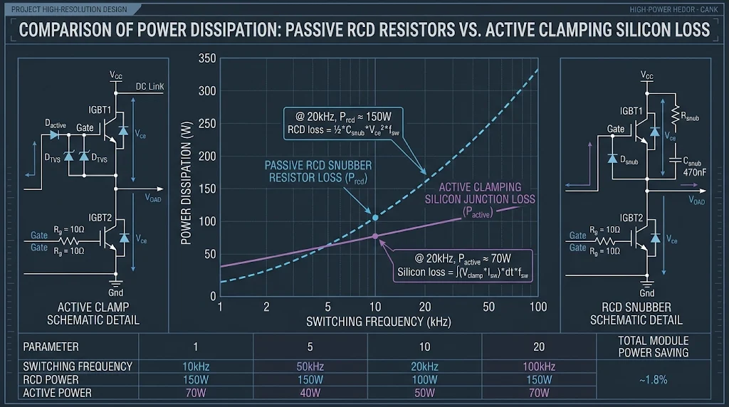
The primary engineering compromise of the passive snubber is continuous thermal loss. In an RCD configuration, the minimum power dissipation in the snubber resistor scales directly with switching frequency (fsw), the snubber capacitance (Cs), and the voltage swing:
Psnubber ≈ k × Cs × ΔV2 × fsw
This expression serves as an engineering estimation under complete charge-discharge cycling conditions, where the topological factor k typically ranges between 0.5 and 1.0 depending on the specific snubber configuration (such as individual switch snubbers versus bridge-leg DC-bus clamp topologies); specific RCD variants or incomplete discharge profiles will exhibit distinct loss characteristics and must not be treated identically.
In high-frequency industrial drives operating above 10 kHz to 20 kHz, sizing Cs for tight voltage clamping can generate substantial continuous thermal dissipation (for instance, tens of watts per phase leg depending on the bus voltage and capacitance value), requiring dedicated thermal budgeting. For a comprehensive mathematical derivation of this efficiency penalty and capacitance optimization trade-offs, explore our specialized study on Snubber Loss Balancing: Navigating the Trade-Off Between Snubber Capacitor Selection and Efficiency Loss.
3. Active Clamping Architecture: Direct Feedback, TVS Avalanche, and Silicon Channel Conduction
Active clamping departs entirely from external capacitive shunting. Instead of diverting energy into a passive tank, active clamping operates by momentarily forcing the IGBT back into its active (linear) conduction region whenever the collector-emitter voltage threatens to exceed a predetermined threshold.
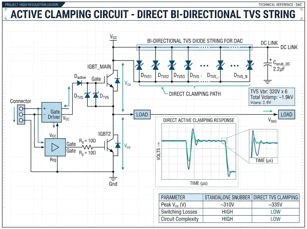
The core of an active clamping circuit consists of a chain of fast transient voltage suppression (TVS) diodes or Zener diodes connected directly between the collector terminal and the gate terminal (or the gate driver feedback node). Under normal operation, the TVS chain remains fully non-conductive, drawing minimal standby leakage current, the exact magnitude of which is governed by the specific TVS diode selection, cumulative DC bias, and operating junction temperature. However, as the collector-emitter voltage surges during rapid turn-off and reaches the cumulative breakdown voltage (VTVS) of the diode string, the TVS diodes avalanche into conduction:
In a direct active clamping (DAC) topology employing a dedicated series damping resistor (Rclamp), the resulting avalanche feedback current is governed by:
Iclamp = (VCE – VTVS – VGE) / Rclamp
This avalanche current (Iclamp) flows directly into the IGBT gate, charging the input gate-emitter capacitance (Cies) and lifting the gate voltage above the gate threshold (VGE(th)). As VGE rises, the IGBT partially re-activates its conduction channel. The device acts as a high-voltage dynamic linear sink, maintaining the collector current required to satisfy the inductor loop while dynamically pinning the collector voltage to a fixed plateau:
VCE(clamp) ≈ VTVS + VGE(th) + Iclamp × Rclamp
This closed-form formulation represents a theoretical first-order approximation under direct feedback. In practical converter operation, the effective clamped plateau voltage is additionally shaped by the IGBT transfer characteristics and forward transconductance (gfs), device junction temperature, Miller capacitance dynamics, and the dynamic sinking impedance of the active gate driver circuit.
Crucially, because active clamping forces the IGBT to conduct collector current while simultaneously sustaining near-breakdown terminal voltage, the dynamic trajectory must remain strictly within the manufacturer’s Reverse Bias Safe Operating Area (RBSOA) and adhere to transient thermal impedance (Zth(j-c)) limitations. Operating outside the dynamic RBSOA during active clamping risks instantaneous device destruction from dynamic avalanche and localized second breakdown.
Once the magnetic energy stored in Lstray has fully dissipated, the collector current drops to zero, VCE settles back to the DC-link voltage, the TVS diodes extinguish, and the gate driver pull-down transistor completes the full turn-off transition.
4. The Hidden Silicon Cost: Junction Temperature Rise During Repeated Active Clamping
The primary advantage of active clamping is high operational efficiency under normal load: because no clamping action occurs when VCE remains below VTVS, continuous parasitic losses are virtually zero. However, active clamping is not lossless; it simply transfers the energy dissipation from an external snubber resistor directly into the IGBT silicon die.
During the transient active clamping interval (Δtclamp, the duration of which is governed dynamically by the commutation loop energy ½LstrayI2 and the voltage clamping headroom), the IGBT simultaneously sustains high collector current (IC) and peak clamped voltage (VCE(clamp)). The total thermal energy dumped into the silicon junction during a single clamping event is given by:
Eclamp = ∫0Δtclamp [VCE(clamp) × iC(t)] dt ≈ ½ × Lstray × Iturn-off2 × [VCE(clamp) / (VCE(clamp) – VDC)]
This closed-form energy expression represents a theoretical first-order approximation, predicated on an idealized constant voltage clamping plateau and a linear collector current fall profile; real-world non-linear tail currents and dynamic avalanche impedances will modulate the actual energy partitioning.
This energy adds directly to the standard turn-off switching energy (Eoff). If an inverter is designed such that active clamping triggers on every standard switching pulse, the continuous thermal dissipation inside the module increases sharply. More critically, the high instantaneous power dissipation concentrated within the active die area during the clamping pulse can induce severe localized transient junction temperature spikes (ΔTj).
Thermal fatigue caused by repeated ΔTj cycling is widely recognized to accelerate bond-wire degradation and solder layer fatigue under the semiconductor die. As established in application notes from major power semiconductor manufacturers such as Infineon Technologies, continuous repetitive active clamping is strongly discouraged for continuous operation; rather, it should serve as an emergency safety net for dynamic overloads, dead-time skew, and short-circuit faults.
5. Gate Driver Demands: Current Sinking, Desaturation Blanking, and Clamping Sizing
Implementing active clamping introduces severe design challenges for the isolated gate driver circuitry. When the TVS string avalanches, it injects current directly into the gate node. At the same time, the gate driver is actively commanding a turn-off, attempting to sink current through its low-side output MOSFET (Rsink) to the negative supply rail (e.g., -8 V or -15 V).
If the gate driver output impedance is too low, it will sink the TVS clamp current to the negative gate-drive rail before VGE can rise sufficiently to modulate the IGBT channel, rendering the active clamp ineffective. Conversely, if the driver impedance is too high, the gate can be overdriven, leading to prolonged current dwell and thermal runaway. Modern gate drive designs resolve this conflict through two primary configurations:
- Direct Active Clamping (DAC): The TVS string feeds current directly to the gate pin, requiring a series feedback resistor (Rclamp) to buffer against the gate driver sink stage. While conceptually simple, the TVS diodes must withstand peak transient currents of several amperes, necessitating physically large TVS packages with high surge ratings.
- Active Clamping with Driver Feedback (Advanced DAC): The TVS cathode connects to the collector, but the anode feeds into an auxiliary high-impedance sense pin on an intelligent gate driver IC, such as isolated drivers outlined in Texas Instruments isolated gate driver architectures. Upon sensing TVS breakdown, the driver automatically disables its low-side sink MOSFET, allowing the gate to float or actively controlling the turn-off slope through an integrated soft turn-off (STO) pull-down stage.
6. Comparative Engineering Matrix: Active Clamping vs. Passive RCD Snubbers
To assist system architects in selecting the optimal overvoltage suppression methodology for industrial motor drives, solar central inverters, and battery energy storage converters, the following trade-off matrix contrasts active clamping against passive RCD snubber architectures:
| Engineering Parameter | Passive RCD Snubber | Active Gate Clamping (DAC) |
|---|---|---|
| Continuous Efficiency Loss | High: Scales continuously with Cs, VDC2, and switching frequency. | Negligible: Near-zero loss during normal operation when VCE < VTVS. |
| Silicon Thermal Stress | Low: Energy is dissipated in external resistors, keeping module Tj cooler. | High: Dissipates clamping energy directly in the IGBT silicon junction during events. |
| Physical Footprint & Weight | Bulky: Requires high-voltage film capacitors, power resistors, and heatsink area. | Minimal: Compact TVS diode string mounted directly on the gate drive PCB. |
| Transient Response Speed | Dependent on snubber diode forward recovery (tfr) and parasitic lead ESL. | Fast: Inherently fast TVS avalanche response, though overall loop clamping dynamics remain constrained by PCB trace parasitics, package ESL, and driver sink impedance. |
| Protection Under Short-Circuit | Conditional: Clamping effectiveness during high-energy fault interruptions depends heavily on the specific snubber topology, capacitor energy capacity, and fault current duration; excessive fault energy may drive capacitor voltage upward and restrict further overvoltage suppression. | Dynamic Overvoltage Limiting: Clamps transient spikes during high-current fault turn-off (must be coordinated with primary desaturation and soft turn-off protection; cannot substitute for short-circuit trip mechanisms). |
| Design Complexity & Tuning | Moderate: Straightforward R and C calculation with parasitic damping verification. | High: Requires precise TVS thermal matching and gate driver sink impedance balance. |
| Primary Application Domain | Continuous high-frequency ringing damping; systems with fixed, predictable loads. | Emergency fault protection, traction inverters, and high-power utility-scale stacks. |
7. Hybrid Clamping Strategies for Fault-Under-Load and Short-Circuit Events
Given the complementary trade-offs between passive and active architectures, elite power electronics designs increasingly implement a coordinated hybrid protection strategy rather than relying on an isolated approach.
In a hybrid architecture, a compact, low-capacitance DC-link bus snubber (or small localized RC snubber) is placed across the power terminals to dampen high-frequency ringing caused by busbar parasitics and diode reverse recovery. This passive element handles the routine, repetitive low-energy micro-transients, preventing high-frequency EMI from interfering with sensitive control circuits.
Concurrently, an active clamping network is integrated onto the gate drive PCB, calibrated with a clamping threshold derived from the nominal peak switching envelope, module VCES ratings, TVS manufacturing breakdown tolerances, and dynamic temperature drift. Under routine inverter modulation, the active clamp remains completely dormant, eliminating silicon thermal penalties. However, when an acute fault occurs—such as a dead-time violation shoot-through, a phase-to-ground short, or a sudden loss of load during peak power delivery—the active clamp immediately intercepts the catastrophic spike, keeping VCE safely clamped while the intelligent gate driver initiates a controlled soft turn-off sequence.
8. Implementation Guidelines and Practical Component Selection
When implementing active clamping or passive snubber circuits in industrial power converter prototypes, engineers should adhere to four fundamental layout and component selection guidelines:
- TVS Temperature Coefficient Compensation: Silicon avalanche TVS diodes exhibit a positive temperature coefficient of breakdown voltage (an illustrative design range is often on the order of ~0.08% to ~0.11% per °C, though exact coefficients vary across diode technologies and must be obtained directly from specific manufacturer datasheets). In a theoretical design scenario, for instance, a TVS diode string with a nominal 1000 V breakdown at a 25 °C reference temperature can shift upward toward ~1100 V as internal TVS junction temperature (Tj(TVS)) surges to 125 °C during repetitive or high-energy clamping events. Designers must evaluate maximum transient junction temperatures (Tj(TVS)) rather than relying solely on ambient specifications, verifying that peak thermal clamping plateaus remain securely within the module VCES envelope.
- Minimizing TVS Loop Parasitic Inductance: The connection from the IGBT collector to the TVS cathode must have minimal loop area. Any parasitic inductance in the active clamp feedback trace delays the injection of gate charge, creating a destructive voltage overshoot before the clamp can engage.
- Snubber Diode Forward Recovery (tfr): In passive RCD networks, standard fast recovery diodes exhibit a forward recovery voltage overshoot (VFRM) during the first few tens of nanoseconds of high di/dt turn-on. Rather than relying solely on generic fast-recovery ratings, circuit designers should verify the snubber diode forward recovery characteristics against the application anticipated rate of current rise (di/dt) to limit additional transient voltage overshoot along the snubber diode conduction path.
- Verified Module Sourcing: Clamping protection can only succeed if the underlying semiconductor modules maintain fully traceable factory origin, consistent lot-to-lot manufacturing quality, and verified safe operating areas (SOA). As an established distributor with over 15 years of industry experience, Shunlongwei Co. Ltd. supplies genuine, fully traceable IGBT modules, low-inductance bus capacitors, and gate drive components from world-leading manufacturers for demanding industrial deployments.