The rapid transition toward Hybrid Electric Vehicles (HEV) and pure Electric Vehicles (EV) has fundamentally reshaped the landscape of power electronics. At the heart of this revolution is the traction inverter, a critical subsystem responsible for converting direct current (DC) from the high-voltage battery into alternating current (AC) to drive the electric traction motor. As automotive manufacturers demand higher power densities, extended driving ranges, and unparalleled long-term reliability, traditional power semiconductor packaging technologies have reached their physical and thermal limits.
To overcome these bottlenecks, the industry has turned to advanced packaging methodologies. Among the most transformative innovations is Double-Sided Cooling (DSC) packaging combined with Solderable Front Metal (SFM) technology and ultra-thin semiconductor chips. This article provides a deep dive into the engineering principles behind these technologies, exploring how the elimination of traditional wire bonds and the integration of 70 μm thin wafers are redefining the reliability boundaries of power modules, enabling ultra-compact 200 kVA power ratings for modern HEV and EV electric drive systems.
What is Double-Sided Cooling (DSC)?
Double-Sided Cooling (DSC) is an advanced power module packaging technology that eliminates traditional top-side wire bonds, replacing them with a planar sandwich structure that allows thermal energy to be extracted from both the top and bottom surfaces of the semiconductor chip simultaneously.
According to documented application benchmarks from leading automotive semiconductor power innovators, implementing a robust wirebond-less DSC packaging scheme yields immediate system-level benefits:
- Power Density Increase: Boosts the current-carrying and power delivery capability by up to 30% to 40% within the same physical inverter footprint.
- Thermal Resistance Mitigation: Significantly reduces the overall junction-to-fluid thermal resistance (RthJF) by establishing an independent, highly conductive secondary cooling path.
- Elimination of Wire Fatigue: Completely obliterates the failure modes associated with traditional heavy aluminum wire bonds, such as heel cracking and lift-off.
- Enhanced Mechanical Ruggedness: Distributes thermo-mechanical stresses symmetrically across the active die area, ensuring compliance with demanding automotive mission profiles.
Understanding the Thermal and Mechanical Challenges in EV Traction Inverters
Power semiconductors, primarily Insulated Gate Bipolar Transistors (IGBTs) and Silicon Carbide (SiC) MOSFETs, generate substantial heat during operation due to switching and conduction losses. In automotive applications, these components are subjected to harsh mission profiles, experiencing continuous and extreme temperature fluctuations. This phenomenon is known as thermal cycling and power cycling.
The fundamental reliability challenge in power module design stems from the Coefficient of Thermal Expansion (CTE). CTE is a material property that quantifies how much a material expands or contracts in response to a change in temperature. A typical power module is a complex multi-layered structure comprising materials with vastly different CTE values. For instance, the silicon (Si) die has a CTE of approximately 2.6 ppm/K, whereas the aluminum (Al) used for top-side wire bonds has a CTE of about 23 ppm/K, and the copper (Cu) baseplate sits at roughly 17 ppm/K.
When the module heats up during high-power transients (such as vehicle acceleration) and cools down during coasting, these materials expand and contract at different rates. This CTE mismatch induces severe thermo-mechanical shear stresses at the interfaces between different materials, eventually leading to material fatigue, degradation, and catastrophic failure. To dive deeper into how package designs attempt to mitigate these thermal issues, you can review our technical guide on IGBT Packaging and Reliability.
The Vulnerability of Traditional Wire-Bonded Power Modules
For decades, the standard method for establishing electrical connections to the top side (emitter or source) of a power semiconductor die has been ultrasonic heavy aluminum wire bonding. While cost-effective and highly mature, wire bonding represents the most significant reliability weak point in high-power automotive modules.
Under repeated power cycling, the massive CTE mismatch between the silicon die and the aluminum wire generates immense stress at the bond interface. Over time, this stress manifests in two primary failure mechanisms:
- Heel Cracking: Micro-cracks initiate at the heel of the wire bond (the point where the wire bends upwards from the die surface) due to repeated flexing. As the crack propagates, the cross-sectional area of the wire decreases, leading to localized heating, which accelerates the cracking process until the wire breaks completely.
- Wire Lift-off: The shear stress at the metallurgical junction between the aluminum wire and the top aluminum metallization of the silicon die causes the bond to literally peel away from the chip surface. Once one wire lifts off, the current redistributes to the remaining wires, increasing their thermal load and causing a rapid cascading failure.
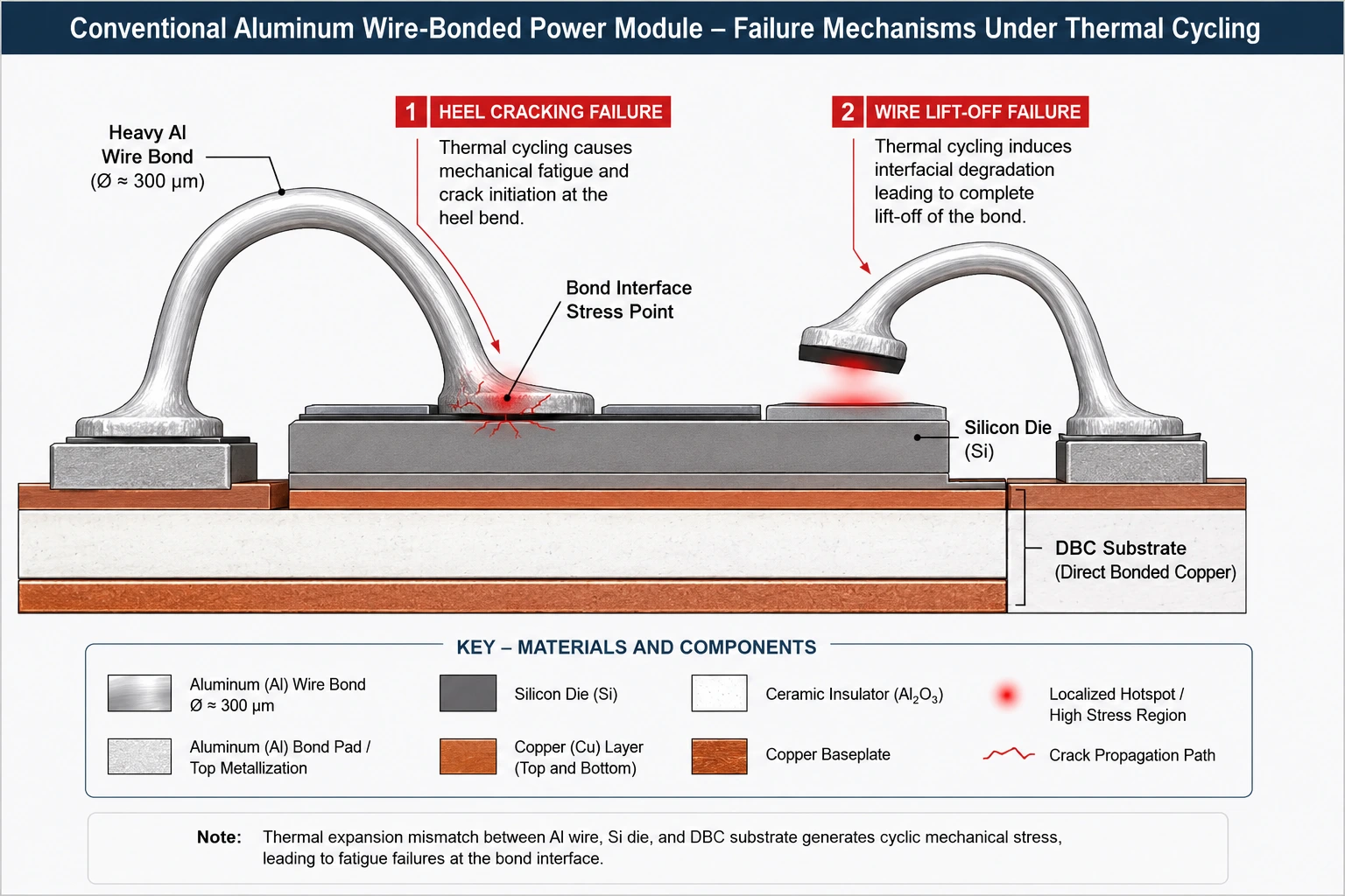
Furthermore, wire bonds introduce significant parasitic inductance. In fast-switching applications, high parasitic inductance (Lstray) combined with high current change rates (di/dt) generates massive voltage overshoots (V = L × di/dt), which can exceed the breakdown voltage of the semiconductor device. To push power modules into the 200 kVA range for compact HEV/EV systems, the industry had to engineer a solution that completely eliminates wire bonds.
Enter Double-Sided Cooling (DSC) Packaging: A Wirebond-Less Revolution
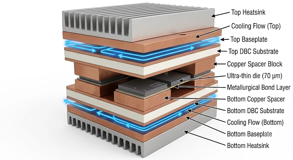
Double-Sided Cooling (DSC) represents a paradigm shift in power module architecture. Instead of relying on wire bonds for the top-side electrical connection and restricting heat dissipation strictly to the bottom of the module, DSC packaging utilizes planar metallic interconnections on both the top and bottom of the semiconductor die. For a broader perspective on this architectural shift, explore our comprehensive topic covering DSC Thermal Management.
In a typical DSC structure, the semiconductor die is sandwiched between two Direct Bonded Copper (DBC) substrates or copper lead frames. Electrical connections to both the collector/drain (bottom) and emitter/source (top) are achieved through large-area metallurgical bonds, such as soldering or silver sintering. This structural innovation delivers two profound advantages:
- Enhanced Thermal Performance: Heat is extracted from both sides of the chip simultaneously. The top-side copper spacer and substrate act as a secondary thermal pathway, dramatically lowering the junction-to-fluid thermal resistance (RthJF). Verified engineering data from International Rectifier indicates that this dual-path cooling configuration successfully drives massive power dissipation while protecting the active area.
- Elimination of Wire Bond Failures: By replacing thin aluminum wires with large-area copper spacers and planar solder/sinter joints, the localized stress points that cause wire lift-off are completely removed. The planar connection evenly distributes thermo-mechanical stresses across the entire chip surface.
However, implementing DSC requires overcoming a massive manufacturing hurdle: standard silicon power chips feature an aluminum top metallization layer optimized specifically for ultrasonic wire bonding. Aluminum cannot be soldered using conventional lead-free solder alloys. This necessitates a fundamental change at the wafer level.
Solderable Front Metal (SFM) Technology: The Key to Wirebond-Less Interconnection
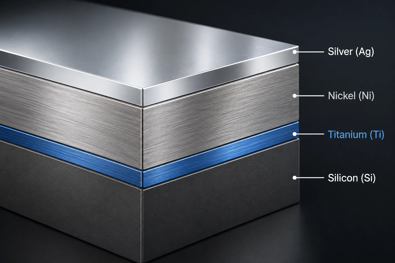
To enable the planar top-side connections required by DSC packaging, semiconductor manufacturers must replace the standard aluminum top layer with a Solderable Front Metal (SFM) system. SFM technology involves depositing a sophisticated multi-layer metallic stack directly onto the active surface of the wafer during the final stages of semiconductor fabrication.
A typical SFM stack consists of several distinct layers, each engineered for a specific physical purpose:
- Adhesion Layer: Usually Titanium (Ti) or Chromium (Cr), this ultra-thin layer ensures robust mechanical adhesion to the underlying silicon and silicon dioxide structures.
- Diffusion Barrier Layer: Often composed of Nickel (Ni) or a Nickel-Vanadium (NiV) alloy. This is the core of the SFM stack. It prevents solder from diffusing directly into the silicon during the high-temperature reflow process, which would otherwise destroy the delicate P-N junctions of the device.
- Oxidation Protection / Wetting Layer: A very thin layer of Silver (Ag) or Gold (Au) is applied as the outermost surface. This layer prevents the underlying nickel from oxidizing when exposed to air and ensures rapid, uniform wetting of the solder alloy or sintering paste during module assembly.
By implementing SFM, engineers can utilize robust soldering or silver sintering processes to attach copper spacers directly to the active area of the IGBT or diode. This large-area metallurgical bond exhibits significantly higher mechanical strength and thermal conductivity than aluminum wire bonds. When subjected to power cycling, the CTE mismatch is managed by the compliance of the solder layer and the structural rigidity of the DBC substrates, pushing the reliability boundaries far beyond the capabilities of wire-bonded modules.
70 μm Ultra-Thin Wafer Technology: Enhancing Electrical and Thermal Performance
While DSC and SFM address the packaging mechanics, the core efficiency of the power module is dictated by the semiconductor die itself. For modern high-density applications, the thickness of the silicon wafer plays a dominant role in both electrical performance and thermal management. Technical datasheets from leading-edge industrial power manufacturers like Infineon demonstrate that modern automotive IGBT modules achieve peak optimization when utilizing ultra-thin chips with thicknesses reduced to an astonishing 70 μm.
Reducing the thickness of an IGBT from a traditional 120 μm down to 70 μm yields immense engineering benefits:
- Reduced Conduction Losses: In an IGBT, the forward voltage drop (VCE(sat)) is highly dependent on the thickness of the n-base drift region. A thinner die means the charge carriers have a shorter distance to travel, significantly reducing the electrical resistance and, consequently, the conduction losses. This translates directly to higher inverter efficiency and longer EV battery range.
- Lower Thermal Resistance: Silicon is a good thermal conductor, but at high power densities, every micrometer of material acts as a thermal barrier. Thinning the die to 70 μm minimizes the bulk thermal resistance of the silicon itself, allowing heat generated at the top surface junctions to travel rapidly to the bottom cooling substrate.
- Improved Switching Characteristics: Ultra-thin wafers hold less stored charge (Qrr) during the conduction phase. Less stored charge means the device can turn off much faster, reducing switching losses (Eoff) and enabling higher frequency operation, which in turn allows for smaller passive components in the system.
Synergizing SFM, Thin Chips, and DSC for Unprecedented Reliability
The true engineering breakthrough occurs when these three technologies—Double-Sided Cooling, Solderable Front Metal, and 70 μm ultra-thin chips—are synergized into a single power module architecture. This combination addresses the core bottlenecks of HEV/EV traction inverters.
In a completely wirebond-less design, the elimination of CTE mismatch-induced wire lift-off removes the most common failure point. The robust planar solder joints enabled by SFM distribute thermo-mechanical stresses evenly. Simultaneously, the 70 μm thin chips generate less heat due to reduced VCE(sat) and allow whatever heat is generated to escape rapidly through both the top and bottom DBC substrates.
The macroscopic result of this micro-level engineering is staggering power density. Utilizing these technologies, power semiconductor manufacturers have successfully developed compact IGBT half-bridge modules capable of delivering 200 kVA in footprints as small as 28.5 mm × 16 mm. This represents a paradigm shift compared to traditional baseplate-mounted gel-filled modules, offering automotive Tier 1 suppliers the ability to shrink the volume and weight of the traction inverter dramatically while simultaneously extending the operational lifespan of the vehicle.
Conclusion
The reliability boundaries of power semiconductor packaging have been thoroughly redefined by the transition away from legacy wire bonding. By addressing the physical realities of CTE mismatch through Solderable Front Metal (SFM) and planar interconnections, and by maximizing thermal and electrical efficiency through 70 μm ultra-thin wafer technology, Double-Sided Cooling (DSC) packaging stands as the pinnacle of modern power electronics engineering.
These innovations enable the creation of ultra-compact, 200 kVA-class power modules that meet the aggressive power density and harsh lifetime requirements of the rapidly expanding HEV/EV market. As the industry also continues to shift towards wide-bandgap materials like Silicon Carbide—a topic deeply explored in our SiC vs. IGBT Comparison—the wirebond-less, double-sided cooling architecture will remain the foundational blueprint for reliable, high-performance electric drive systems.
Frequently Asked Questions
What is Double-Sided Cooling in power modules?
Double-Sided Cooling (DSC) is a structural packaging design where the power semiconductor chip (IGBT or MOSFET) is sandwiched between two direct bonded copper (DBC) substrates. This architecture replaces legacy top-side aluminum wire bonds with large metallic copper spacers, allowing heat to escape through both the top and bottom surfaces simultaneously, doubling the effective heat dissipation area.
Why are wire bonds a reliability concern in automotive inverters?
Wire bonds are prone to thermo-mechanical fatigue due to the severe Coefficient of Thermal Expansion (CTE) mismatch between the aluminum wire (23 ppm/K) and the silicon die (2.6 ppm/K). During the aggressive power cycling profiles typical of an EV (acceleration and regenerative braking), this mismatch induces cyclical shear stresses at the contact pad, causing heel cracking or wire lift-off failures.
How does Solderable Front Metal (SFM) technology work?
Standard power chips feature an aluminum top metallization optimized for ultrasonic wire bonding, which cannot be soldered. SFM technology deposits a multi-layer metallic stack (typically a Titanium adhesion layer, a Nickel diffusion barrier, and a Silver or Gold wetting layer) over the active top surface of the wafer. This modified surface allows large-area planar joints to be formed using traditional soldering or silver sintering.
Why are 70 μm thin wafers used in EV traction modules?
Thinning the silicon wafer down to 70 μm drastically shortens the distance that charge carriers must travel inside the n-base drift region of an IGBT. This significantly lowers the forward conduction voltage drop (VCE(sat)) and reduces bulk thermal resistance. It also minimizes the stored charge (Qrr), leading to faster turn-off times and greatly suppressed switching energy losses (Eoff).
Can DSC technology be used with Silicon Carbide (SiC) MOSFETs?
Yes, DSC technology is highly compatible with and increasingly necessary for SiC MOSFETs. Although SiC chips offer lower switching losses, their physical die size is significantly smaller than equivalent silicon parts for a given current rating. This creates extreme localized heat flux. Implementing wirebond-less DSC packaging provides the necessary dual-path cooling to manage this concentrated heat and exploit SiC’s high-temperature capabilities safely.
Recommended Specific Products for HEV/EV Applications
To successfully implement the high-efficiency, wirebond-less cooling concepts discussed in this article, design engineers must select components engineered for cutting-edge thermal management and extreme power density. Based on the stringent requirements of modern HEV/EV traction inverters, we highly recommend evaluating the following specific power modules:
- COOLiR2BRIDGE™ / COOLiR2DIE™ (650V / 300A): Directly embodying the Double-Sided Cooling (DSC) and Solderable Front Metal (SFM) technologies discussed above, this ultra-compact architecture delivers a 200 kVA power rating in a mere 28.5 mm × 16 mm footprint. It is the definitive choice for severely space-constrained automotive traction inverters requiring maximum thermal efficiency.
- Infineon FF600R12IP4 (1200V / 600A): A proven high-power standard in the industry. For heavy-duty electric commercial vehicles or systems where maximum current handling and rugged thermal cycling are paramount, this dual IGBT module provides exceptional long-term reliability and trench-field-stop performance.
- Infineon CoolSiC™ FS45MR12W1M1_B11 (1200V): If your electric drive design is transitioning to Wide-Bandgap (WBG) technology to maximize driving range, this EasyPACK™ 1B SiC MOSFET module is an excellent choice. It drastically reduces switching losses while accommodating higher junction temperatures, complementing advanced cooling strategies.
For detailed datasheet specifications, thermal impedance curves, and to source the exact semiconductor match for your next-generation traction inverter, explore our comprehensive inventory of advanced power modules and electronic components.