Resonant Topologies in Home Appliances: A Technical Deep Dive into Quasi-Resonant vs. Half-Bridge Series Resonant Induction Heating
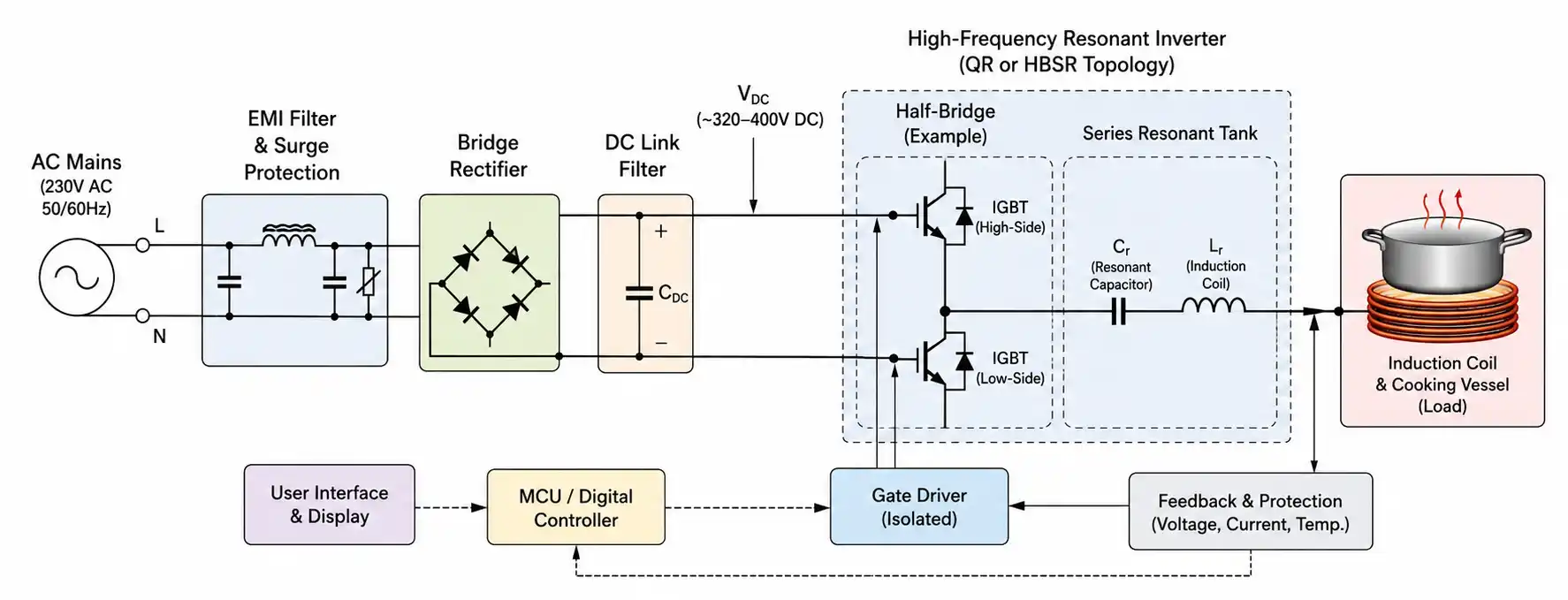
Induction cooking technology has fundamentally transformed the residential and commercial culinary markets by delivering unprecedented energy efficiency, rapid thermal response times, and an inherently safe user experience. Unlike conventional gas or electric radiant cooktops that rely on thermal conduction or radiation to transfer heat from an external source to a cooking vessel, induction heating (IH) systems generate heat directly within the workpiece itself. At the heart of every induction appliance is a high-frequency inverter circuit that orchestrates this energy conversion. For power electronics design engineers, selecting and optimizing the appropriate inverter topology is the most critical decision governing product reliability, thermal performance, and bill-of-materials (BOM) cost.
In modern domestic appliances, two resonant inverter topologies dominate the landscape: the Quasi-Resonant (QR) topology and the Half-Bridge Series Resonant (HBSR) topology. While the QR configuration has long been the industry standard for cost-sensitive single-hob applications, the HBSR topology has emerged as the definitive standard for premium, multi-zone cooktops due to its superior power control granularity and architectural flexibility. This technical article provides an exhaustive comparative analysis of these two prominent paradigms, focusing on their soft-switching mechanisms, voltage stress profiles, control methodologies, and the transformative impact of integrated Reverse-Conducting (RC) Insulated Gate Bipolar Transistors (IGBTs) on system performance.
1. Foundational Electro-Magnetic and Resonant Physics
To accurately evaluate induction inverter topologies, one must first grasp the core multi-physical principles governing the load. An induction cooker operates on the combined principles of Ampere’s Law, Faraday’s Law of Induction, and the Joule Effect. A high-frequency alternating current, typically ranging from 20 kHz to 100 kHz, is forced through a planar copper induction coil. This current generates an oscillating magnetic flux that penetrates the ferromagnetic bottom of the cooking vessel placed directly above it.
The time-varying magnetic field induces eddy currents within the vessel’s base. Because ferromagnetic materials possess substantial magnetic permeability, the high-frequency current is confined to a thin peripheral layer of the vessel floor due to the skin effect. The skin depth is inversely proportional to the square root of the operating frequency, electrical conductivity, and relative permeability. This localized concentration of eddy currents flowing through the surface resistance of the pan base generates immense heat via Joule dissipation (P = I2R). Concurrently, magnetic hysteresis losses within the ferromagnetic material contribute minor additional thermal energy. To fully understand the role of power semiconductors in managing these severe inductive loads, engineers can refer to The Critical Role of IGBTs in Induction Cooking.
Because the induction coil exhibits low electrical resistance and high inductance, driving it directly with a hard-switched inverter would result in catastrophic switching losses and destructive electromagnetic interference (EMI). To overcome this, a resonant tank circuit is formed by pairing the induction coil (acting as a non-ideal transformer with a short-circuited secondary winding) with one or more high-voltage resonant capacitors. By tuning the inverter switching frequency near the natural resonant frequency of this LC network, the system can achieve soft-switching operation, substantially mitigating switching losses.
2. The Quasi-Resonant (QR) Topology: Cost-Optimized Monolithic Switching
The Quasi-Resonant topology represents the most widely deployed inverter architecture in single-burner portable induction cooktops and domestic rice cookers. Its market dominance in these segments is driven primarily by its elegant, minimalistic circuit design, which minimizes component count and overall system cost.
2.1 Circuit Architecture and Operational Phases
A classic QR inverter utilizes a single power semiconductor switch (typically an IGBT) arranged in parallel with a single resonant capacitor, both of which are connected across the induction coil load. The entire network is fed from a rectified and filtered DC bus. The operational sequence of a QR inverter can be segmented into three distinct phases:
- Energy Storage Phase: The IGBT is gated on. The full DC bus voltage is applied across the induction coil电感. The collector current rises linearly, storing energy within the magnetic field of the coil. The resonant capacitor is shorted by the conducting switch.
- Resonant Ringing Phase: The IGBT is commanded off. Because the current through the inductive coil cannot drop instantaneously, the current diverts into the parallel resonant capacitor. The capacitor charges up, and the collector-emitter voltage VCE of the IGBT rises, forming a large half-sinusoidal voltage pulse. Once the stored inductive energy is entirely transferred to the capacitor, the capacitor discharges back through the coil, causing VCE to drop back toward zero.
- Free-Wheeling/Clamping Phase: As VCE rings down and crosses below zero volts, the anti-parallel or integrated freewheeling diode of the IGBT becomes forward-biased. This clamps the voltage across the switch to a negative diode forward drop (-VF) and allows the remaining energy to return to the DC link. It is during this specific clamping interval that the IGBT can be turned back on under Zero Voltage Switching (ZVS) conditions.
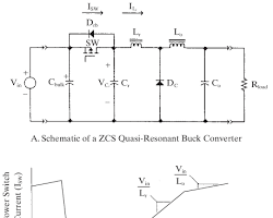
2.2 Soft-Switching (ZVS/ZCS) Dynamics
Achieving True ZVS turn-on requires precise timing from the system microcontroller or specialized control IC. The gate drive pulse must be applied precisely while the freewheeling diode is conducting current in the reverse direction. If the switch is turned on too early or too late, the resonant capacitor will discharge directly through the IGBT channel, causing severe current spikes and excessive turn-on switching losses. Turn-off losses are also naturally limited because the parallel resonant capacitor acts as a turn-off snubber, limiting the rate of rise of the collector-emitter voltage (dV/dt) immediately after the channel is extinguished.
2.3 High-Voltage Stress and Overvoltage Protection (OVP) Challenges
The principal engineering bottleneck of the QR topology is the extraordinary voltage stress imposed on the single power switch. During the resonant ringing phase, the peak collector-emitter voltage VCE(peak) routinely scales to three or four times the input DC bus voltage. For a standard 230V AC residential grid rectified to a ~325V DC bus, the peak resonant voltage across the IGBT frequently exceeds 900V to 1100V.
Under transient grid fluctuations, or when a cooking pan is abruptly lifted from the cooktop (causing a sudden drop in effective magnetic coupling and an increase in load inductance), this resonant peak can easily breach 1200V. Consequently, engineers are forced to specify premium 1200V or 1350V rated power semiconductors for high-frequency designs. Selecting the correct device entails analyzing parameters far beyond simple saturation voltages; details on this process can be explored in this technical resource on IGBT Selection Beyond VCE(sat) for High-Frequency Designs. Furthermore, a robust, ultra-fast Overvoltage Protection (OVP) feedback loop must be implemented to instantly truncate the IGBT turn-on time if the resonant voltage approaches the breakdown threshold, preventing catastrophic overvoltage failure.
3. The Half-Bridge Series Resonant (HBSR) Topology: High-Power Precision
As consumer demand shifts toward multi-burner cooktops and flexible, full-surface induction zones, the Half-Bridge Series Resonant topology has become the preferred choice for high-tier appliance designs. Although it requires a higher initial component count, its electrical performance eliminates many of the inherent limitations of the QR circuit.
3.1 Architecture, Voltage Balancing, and Lower Device Ratings
The HBSR topology comprises two discrete power semiconductor switches (a high-side IGBT and a low-side IGBT) configured in a standard half-bridge phase leg. The output node between the two switches is connected to a series LC resonant tank, consisting of the induction coil and a capacitive divider or single series resonant capacitor connected to the DC bus rails.
The fundamental structural advantage of the half-bridge configuration is that the voltage across the switches is naturally clamped to the DC bus voltage. When the high-side switch is off, the low-side switch or its freewheeling diode clamps the high-side switch voltage to VDC, and vice versa. Therefore, under normal operating conditions on a 230V AC mains supply, the maximum voltage stress across either IGBT never exceeds the rectified bus voltage of approximately 325V to 400V. This enables power electronics engineers to utilize highly optimized 600V or 650V rated IGBTs instead of the expensive, high-voltage 1200V/1350V components mandated by QR systems. This reduction in required voltage rating enables the use of thinner semiconductor drift regions, which dramatically lowers conduction losses.
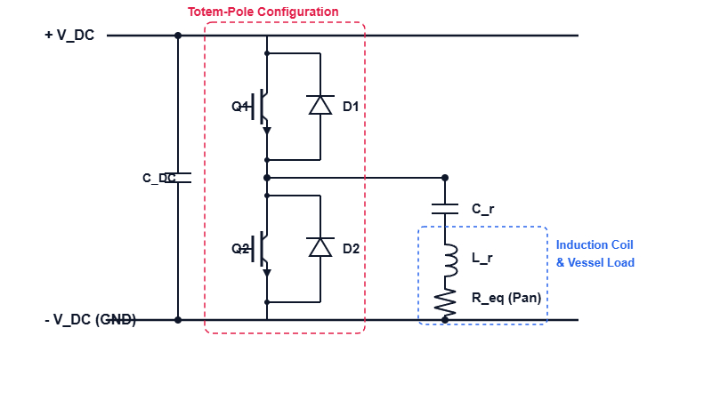
3.2 Advanced Power Modulation via Frequency Control
Power control in an HBSR circuit is accomplished through Variable Frequency Modulation (VFM) or Pulse Width Modulation (PWM) with fixed or asymmetrical duty cycles. The most reliable control technique involves operating the half-bridge at a switching frequency slightly above the resonant frequency of the LC tank. Because the circuit operates in the inductive region of the resonance curve, the current lags the voltage.
When an active IGBT turns off, the lagging inductive current naturally discharges the parasitic output capacitance of the opposing switch and charges the capacitance of the off-going switch. This forces the voltage across the oncoming switch to reach zero before its gate drive signal is applied, establishing reliable ZVS across the entire power range. This smooth control mechanism is critical to preventing sudden thermal and electrical overstress, as documented in IGBT Failure Analysis: Preventing Overcurrent, Overvoltage, and Overtemperature.
3.3 Eliminating Low-Power Acoustic and Burst-Mode Drawbacks
A classic flaw of the Quasi-Resonant topology is its inability to deliver continuous, smooth low-power heating. To output low power (e.g., for simmering delicate sauces), a QR system must resort to “burst mode” control—turning the entire inverter on and off at low frequencies (e.g., 1 Hz to 2 Hz). This causes intermittent boiling and can lead to uneven cooking.
Conversely, the HBSR topology can easily scale its power output continuously from maximum wattage down to very low levels by adjusting the switching frequency further up the inductive slope or employing phase-shift control. Furthermore, in multi-hob appliances, if adjacent hobs operate at independent, un-synchronized high frequencies, the magnetic coupling between coils can generate audible intermodulation noise (acoustic beat frequencies). The HBSR topology permits simple synchronization of the switching clocks across multiple hobs, completely eliminating this user-experience drawback.
4. Comprehensive Topological Comparison Matrix
To assist design engineers in evaluating tradeoffs, the following matrix summarizes the technical discrepancies between the two resonant paradigms:
| Architectural Parameter | Quasi-Resonant (QR) Inverter | Half-Bridge Series Resonant (HBSR) Inverter |
| Power Switch Count | 1 Discrete or Integrated IGBT | 2 IGBTs in a Half-Bridge Configuration |
| IGBT Voltage Rating (Mains 230V AC) | 1200V to 1350V required due to resonance spikes | 600V to 650V clamped to the maximum DC bus |
| Resonant Voltage Stress | Extremely High (VCE spikes up to 1200V) | Low (Naturally limited to VDC bus voltage) |
| Low-Power Performance | Discontinuous Burst Mode (On/Off cycling) | Continuous Frequency Modulation down to minimal power |
| Acoustic Beat Noise Susceptibility | High in multi-burner systems; difficult to sync | Very Low; easily synchronized across multi-burner systems |
| Relative Gate Driver Complexity | Low (Single low-side referenced driver) | High (Requires high-side floating bootstrap or isolated driver) |
| Relative System Bill-of-Materials Cost | Minimal (Highly cost-optimized) | Moderate to High (Requires extra switch, driver, and caps) |
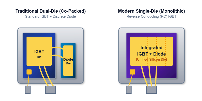
5. The Paradigm Shift: Reverse-Conducting (RC) IGBTs in Induction Heating
Regardless of whether a QR or HBSR topology is selected, the overall efficiency, power density, and reliability of the appliance are governed by the underlying power semiconductor technology. Historically, engineers utilized a discrete co-packed solution consisting of a standard IGBT die placed alongside a separate fast-recovery freewheeling diode within a single package. The advent of Reverse-Conducting (RC) IGBT technology has revolutionized this design approach.
5.1 Monolithic Device Physics vs. Co-Packed Alternatives
An RC-IGBT integrates the freewheeling diode directly into the IGBT silicon structure on a single monolithic die. By embedding n-doped regions into the p-doped collector layer at the back side of a Trenchstop vertical IGBT structure, the device functions as an IGBT when biased in the forward direction and acts natively as a pin diode under reverse bias conditions.
This monolithic integration eliminates the separate diode die entirely. The space savings achieved on the silicon level directly translate into reduced package dimensions or a significantly expanded active silicon area within standard packages like TO-247. This compact integration requires specialized driving consideration; engineers can learn more about managing gate charge dynamics in 5 Practical Tips for Robust IGBT Gate Drive Design.
5.2 Conduction and Switching Loss Optimization
Modern RC-IGBTs tailored specifically for resonant induction applications are engineered to achieve an optimal balance between the collector-emitter saturation voltage VCE(sat) and the forward voltage drop VF of the integrated diode. In a QR inverter, conduction losses are shared between the IGBT channel during the energy storage phase and the diode during the free-wheeling phase.
By utilizing advanced field-stop trench topologies, the latest RC-IGBT generations dramatically reduce the carrier storage effect in both forward and reverse conduction modes. This minimizes the turn-off tail current of the IGBT and lowers the reverse recovery charge Qrr of the integrated diode, reducing total power dissipation at switching frequencies above 25 kHz.
5.3 Thermal Dynamics and the Engineering Path to Silent, Fanless Systems
One of the most profound engineering advantages of monolithic RC-IGBT integration lies in its superior thermal behavior. In a conventional co-packed solution, the IGBT and diode dies act as two concentrated thermal sources. During periods of intense freewheeling or high-power conduction, one die can experience localized overheating while the other remains relatively cool, leading to severe thermal gradients across the package substrate.
In an RC-IGBT, because the diode functionality is distributed uniformly across the entire chip area, the entire silicon surface acts as a heat dissipator regardless of whether the device is conducting in forward or reverse mode. This significantly lowers the effective transient thermal impedance from the junction to the case, denoted as Rth(j-c). For an in-depth analysis of how managing this parameter influences long-term reliability, see Why Rth Matters: Unlocking IGBT Thermal Performance.
By reducing peak junction temperatures and eliminating hot spots, the thermal stress on the system heat sink is drastically reduced. This allows design engineers to downscale the volume and mass of the aluminum extrusion heat sinks. In medium-power appliances or premium induction rice cookers, this thermal optimization enables the complete elimination of forced-air cooling fans. Transitioning to a natural convection, fanless thermal design yields two massive market advantages: it eliminates mechanical fan noise, creating completely silent home appliances, and it prevents the internal accumulation of grease and dust that typically shortens the operational lifespan of fan-cooled electronics.
6. Engineering Selection Framework
When starting a new domestic induction design, engineers can navigate the selection process using the following framework:
- Determine Target Power and Price Point: For single-hob appliances under 2.1 kW where lowest manufacturing cost is the primary driver, select the Quasi-Resonant topology paired with a 1350V RC-IGBT. Ensure the microcontroller’s OVP interrupt loop is prioritized to clamp voltage spikes.
- Assess Multi-Hob Multi-Zone Requirements: For premium multi-burner products or configurations exceeding 3 kW, specify the Half-Bridge Series Resonant topology. Utilize optimized 650V RC-IGBTs to take advantage of the lower conduction losses afforded by a thinner drift region.
- Design for Thermal Longevity: Always simulate the junction temperature swing under worst-case pan material scenarios (e.g., lower-grade stainless steel with poor magnetic coupling). Capitalize on the uniform thermal distribution of monolithic RC-IGBTs to optimize heat sink geometry and reduce acoustic signatures.
7. Conclusion
Resonant technology has elevated domestic induction heating to unparalleled heights of efficiency and performance. Choosing between the single-switch simplicity of the Quasi-Resonant topology and the precision control of the Half-Bridge Series Resonant architecture requires balancing BOM cost against performance requirements. As power electronics designs continue to demand higher power densities and ultra-reliable, silent thermal management, modern monolithic technologies like Reverse-Conducting IGBTs will remain indispensable tools for appliance design engineers worldwide.