As any seasoned power electronics engineer will tell you, the sound of an IGBT module failing is unforgettable. It’s a sharp, concussive “pop” that signifies not just the destruction of a costly component, but also project delays, difficult troubleshooting, and a hit to system reliability. While the high-power IGBT module often takes the blame, the real culprit frequently hides in plain sight: the gate driver circuit. This circuit is the brain that commands the IGBT’s brawn. A poorly designed driver is like giving a world-class athlete bad instructions—the result is inevitably poor performance and, in this case, catastrophic failure. Getting the gate drive right is your first and most critical line of defense.
Based on years of analyzing field failures and optimizing designs, here are five practical, field-tested tips for designing a robust IGBT driver circuit that will keep your systems running reliably and prevent that dreaded “pop.”
Tip 1: Master Gate Resistance (Rg) for Optimal Switching Speed
The gate resistor, Rg, is arguably the most fundamental component in a driver circuit, yet its selection is a delicate balancing act. It directly controls how quickly the IGBT’s internal gate capacitance charges and discharges, thus defining the turn-on and turn-off speeds.
The Double-Edged Sword of Gate Resistors
Choosing the value of Rg involves a critical trade-off between switching efficiency and electrical stress:
- Low Rg Value: This allows for rapid charging of the gate, leading to fast switching. The primary benefit is reduced switching losses (Eon and Eoff), which is crucial for high-frequency applications to maintain thermal stability. However, the downside is significant: fast switching creates high dV/dt (rate of change of voltage) and dI/dt (rate of change of current), which can cause severe voltage overshoots and ringing due to stray inductance in the circuit. This can also generate substantial electromagnetic interference (EMI).
- High Rg Value: A larger resistor slows down the switching process. This “softens” the switching, effectively dampening voltage overshoots and reducing EMI. However, it increases the time the IGBT spends in the active region, leading to higher switching losses and potentially requiring a larger heat sink.
Practical Guidance: Separate Turn-On and Turn-Off Resistors
A one-size-fits-all Rg is rarely optimal. In most applications, you want a controlled, slightly slower turn-on to manage dI/dt and turn-on overcurrent, but a very fast turn-off to minimize turn-off losses and reduce the risk of cross-conduction in half-bridge topologies. The solution is to use separate gate resistors for the turn-on (Rg_on) and turn-off (Rg_off) paths, typically implemented with a diode.
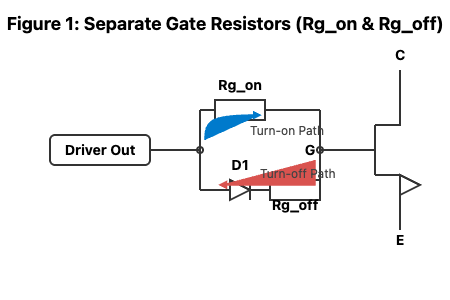
This allows you to select a larger Rg_on to control the turn-on transient and a smaller Rg_off for swift turn-off. Always start with the value recommended in the IGBT module datasheet, such as for the CM600DX-24T, and then use an oscilloscope to fine-tune the values by observing the gate voltage waveform and the collector-emitter voltage (Vce) for overshoots.
Tip 2: Implement a Negative Gate Voltage for Robust Turn-Off
Many designers mistakenly believe that a 0V gate voltage is sufficient to keep an IGBT turned off. In a high-stress power environment, 0V is not truly “off” and leaves the system vulnerable to a destructive phenomenon known as parasitic turn-on.
Why 0V Isn’t “Off” Enough: The Miller Capacitance Threat
The problem lies with the Miller capacitance (Cgc), the capacitance between the gate and the collector. In a typical half-bridge, when one IGBT (let’s say the low-side) turns on, a very high dV/dt is applied across the high-side IGBT, which is supposed to be off. This rapidly changing voltage induces a current that flows through the high-side IGBT’s Miller capacitance and into its gate resistor. This current creates a voltage drop across Rg, causing the gate-emitter voltage (Vge) to spike. If this spike exceeds the IGBT’s gate threshold voltage (Vth), the “off” device will momentarily turn on, creating a direct path between the positive and negative DC rails—a catastrophic shoot-through event.
The Solution: Applying a Negative Bias (-5V to -15V)
The professional solution is to apply a negative voltage to the gate during the off-state. Instead of aiming for 0V, the driver pulls the gate down to a negative potential, typically between -5V and -15V. For example, using a -8V bias means the parasitic voltage spike must now climb from -8V all the way past Vth (e.g., +6V), requiring a much larger energy injection. This provides a robust safety margin against parasitic turn-on. This is a standard and essential practice for reliable gate drive design, especially in motor drives and high-frequency inverters. A proper understanding of IGBT failure modes is crucial, as detailed in our guide on preventing common IGBT failures.
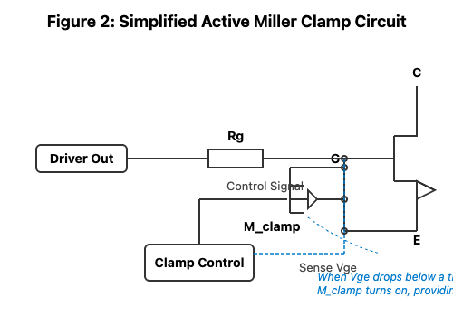
Tip 3: Use an Active Miller Clamp for Absolute Turn-Off Security
In applications with extremely fast switching speeds or very high bus voltages, even a negative gate bias may not be enough to prevent parasitic turn-on. For these mission-critical designs, an Active Miller Clamp provides an additional layer of robust protection.
How an Active Miller Clamp Works
An Active Miller Clamp is a circuit that provides a very low-impedance path from the IGBT’s gate to its emitter *after* it has been turned off. The clamp is intelligently controlled:
- During normal turn-off, the gate driver pulls the gate voltage down towards the negative rail.
- Once the gate voltage drops below a safe threshold (e.g., 2V), the clamp circuit activates a small, auxiliary MOSFET.
- This auxiliary MOSFET directly shorts the IGBT’s gate to its emitter (or the negative supply rail).
This creates a powerful, low-impedance shunt that diverts any current induced by the Miller effect, effectively “clamping” the gate voltage and preventing it from rising. It’s a proactive defense that ensures the IGBT remains securely off, no matter how severe the dV/dt from the opposing device. Many modern gate driver ICs from manufacturers like Infineon now integrate this critical feature.
Tip 4: Design Robust Desaturation (DESAT) Protection
Desaturation is the precursor to nearly every short-circuit-induced IGBT explosion. A robust desaturation (DESAT) protection circuit is not a luxury; it’s an absolute necessity for system survival.
Detecting the Onset of Disaster
In normal operation, a turned-on IGBT is in “saturation,” meaning it has a very low collector-emitter voltage (Vce(sat)), typically 1-3V, even with hundreds of amps flowing through it. During a short-circuit or severe overload, the collector current (Ic) skyrockets. The IGBT can no longer maintain saturation, and its Vce rapidly increases. This condition, with both high current and high voltage simultaneously present, results in an enormous and instantaneous power dissipation (P = Vce * Ic) that will destroy the silicon die in microseconds. Most datasheets specify a Short-Circuit Withstand Time of only 5-10µs.
The DESAT Protection Circuit in Action
A DESAT protection circuit works by monitoring the IGBT’s Vce:
- A high-voltage diode is connected to the IGBT’s collector. During normal operation, Vce is low, and this diode is reverse-biased.
- A constant current source attempts to charge a small capacitor. When Vce rises during a DESAT event, the monitoring diode becomes forward-biased.
- This event triggers a comparator inside the gate driver IC, which registers a fault. To prevent false trips during the normal turn-on transition, a “blanking time” is implemented, during which the DESAT detection is ignored.
- Once a fault is confirmed, the driver initiates a “soft turn-off” (a controlled, slower turn-off) to avoid huge voltage overshoots from rapidly interrupting the massive fault current. It also sends a fault signal to the system’s microcontroller.
This protection is the difference between a controlled system shutdown and a shower of sparks.
Tip 5: Minimize Stray Inductance with Smart PCB Layout
An engineer can follow the first four tips perfectly, but a poor PCB layout can undo all of it. Parasitic inductance, the “hidden” inductance in every PCB trace and component lead, is a primary source of voltage overshoot that can kill an IGBT.
The Hidden Killer: Parasitic Inductance
The key equation is V = L * (dI/dt). The stray inductance (L) in the high-frequency commutation loop (from the DC-link capacitor, through the IGBT, and back) is critical. During the fast turn-off of a large current (high dI/dt), this inductance generates a voltage spike (V) that adds to the bus voltage. This combined voltage can easily exceed the IGBT’s breakdown voltage rating (Vces), leading to avalanche breakdown and failure.
PCB Layout Best Practices
- Minimize Loop Area: This is the golden rule. Keep the high-current paths as short and wide as possible. The outgoing and return paths should be layered directly on top of each other to maximize flux cancellation and minimize the inductive loop area. For high-power modules, laminated busbars are the industry standard.
- Place the Driver Close: The gate driver circuit must be physically located as close as possible to the IGBT module’s gate and emitter pins. Long traces add inductance and make the gate signal susceptible to noise.
- Use Kelvin Emitter Pins: Many modern power modules, like the FF450R12KE4, provide a separate “Kelvin Emitter” connection. This pin is used exclusively as the reference for the gate driver return path. It connects directly to the emitter on the silicon die, bypassing the main load current path and its associated stray inductance. This ensures the driver provides a clean, precise Vge signal, unaffected by voltage fluctuations on the power emitter. The benefits are well-documented by leading manufacturers. You can learn more about this crucial feature from resources like this Kelvin Emitter guide.
- Strategic Decoupling: Place high-quality, low-ESR/ESL ceramic decoupling capacitors directly at the gate driver’s power supply pins and as close as possible to the IGBT module’s main DC input terminals. This provides a local source of high-frequency current, reducing the effective commutation loop size.
Summary: A Checklist for a Robust IGBT Driver Design
Preventing IGBT failure is a matter of systematic, defensive design. The gate driver is the heart of this strategy. By investing engineering effort into these key areas, you significantly enhance system reliability and longevity.
| Design Tip | Key Action | Benefit |
|---|---|---|
| 1. Gate Resistance (Rg) | Use separate Rg_on and Rg_off values. Start with datasheet recommendations and tune with an oscilloscope. | Balances switching speed, losses, and EMI/overshoot control. |
| 2. Negative Gate Voltage | Implement a negative bias (e.g., -8V) for the off-state. | Provides a robust margin against parasitic turn-on caused by the Miller effect. |
| 3. Active Miller Clamp | Add a clamp circuit to short the gate to emitter after turn-off. | Offers ultimate protection against dV/dt-induced turn-on in high-speed systems. |
| 4. Desaturation Protection | Implement a Vce-monitoring circuit with blanking time and soft turn-off. | Detects short circuits within microseconds and enables a safe, controlled shutdown. |
| 5. Smart PCB Layout | Minimize commutation loop area and place the driver close to the IGBT. Use Kelvin Emitter pins. | Reduces parasitic inductance, preventing destructive voltage overshoots during switching. |
A well-designed driver circuit is a critical investment that ensures the expensive IGBT modules you specify can perform to their full potential safely. For your next high-reliability project, explore our extensive range of IGBT modules and compatible driver solutions. Our expert engineering team is ready to help you select the perfect components to build a truly robust system. Contact us at SLW-ELE.COM for technical support and sourcing.