Gate Resistor (Rg) Selection: The Art of Balancing IGBT Switching Speed and Stability (2025 Q4)
The Critical Role of the Gate Resistor (Rg) in IGBT Performance
In the world of power electronics, the Insulated Gate Bipolar Transistor (IGBT) is a cornerstone of modern high-power conversion systems. Yet, for all its power, its performance hinges on a deceptively simple component: the gate resistor (Rg). Many engineers, under pressure to meet deadlines, either default to the value recommended in the datasheet or are tempted to use the smallest possible resistance to maximize switching speed. This seemingly minor decision can be the hidden cause of major design headaches, including catastrophic device failure, excessive electromagnetic interference (EMI), and frustrating system instability.
The gate resistor is far more than a simple current-limiter. It is the primary control knob for the dynamic behavior of the IGBT. Choosing its value is a delicate balancing act—a true engineering art form. Go too low, and you risk violent voltage overshoots and oscillations that can destroy the device. Go too high, and you suffer from excessive switching losses, leading to overheating and poor system efficiency. This article provides a comprehensive, practical guide for engineers to master the selection of Rg, moving from guesswork to a deliberate, system-aware design process.
Understanding the Core Trade-Off: Speed vs. Stability
The fundamental conflict in gate drive design is between switching speed and operational stability. The gate resistor is the fulcrum on which this balance rests. To understand this, we must look at how Rg directly influences the rates of change of current (dI/dt) and voltage (dV/dt) during switching transitions.

How Rg Controls Switching Speed (dI/dt and dV/dt)
An IGBT’s gate behaves like a capacitor, primarily defined by its input capacitance (Cies), which is the sum of the gate-emitter capacitance (Cge) and the gate-collector capacitance (Cgc), also known as the Miller capacitance. The gate driver’s job is to charge and discharge this capacitance to turn the IGBT on and off. The gate resistor, Rg, forms an RC circuit with Cies, dictating the charging and discharging current.
- Low Rg Value: A smaller gate resistor allows a higher peak current to flow from the gate driver. This charges the input capacitance more quickly, resulting in faster turn-on and turn-off times. The immediate benefits are lower switching losses (Eon and Eoff), which is critical in high-frequency applications like welding power supplies and solar inverters to maximize efficiency and minimize heat sink size.
- High Rg Value: A larger gate resistor limits the gate current, slowing down the charging and discharging of Cies. This leads to longer switching transitions, increasing switching losses and generating more heat within the IGBT module.
The Dark Side of Speed: Instability and EMI
While fast switching seems ideal, it comes with significant risks rooted in the parasitic elements of the power circuit. Every wire, PCB trace, and component lead has parasitic inductance. When current changes rapidly (high dI/dt), this inductance induces a significant voltage spike (V = L * dI/dt).
- Voltage Overshoot (Vce peak): During turn-off, a high dI/dt through the main power loop’s stray inductance causes a large voltage spike across the IGBT’s collector-emitter terminals. If this peak voltage exceeds the IGBT’s breakdown voltage rating (Vces), the device will be permanently damaged.
- Gate Ringing and Oscillation: A fast-changing gate voltage can excite the resonant tank formed by the gate drive loop inductance and the IGBT’s input capacitance. This results in high-frequency ringing on the gate voltage (Vge). Severe ringing can cause the gate voltage to drop below the Miller plateau or even rise above the threshold voltage again, leading to unintended switching events, increased losses, or shoot-through in a half-bridge configuration.
- EMI Generation: High dV/dt and dI/dt are primary sources of electromagnetic interference. These rapid changes radiate energy that can disrupt adjacent control circuits and cause the entire system to fail EMC compliance testing. A slower switching speed, controlled by a larger Rg, is often a necessary measure to mitigate EMI.
Key Factors Influencing Rg Selection
A successful Rg selection requires a holistic view of the IGBT, the gate driver, the physical layout, and the end application. Simply copying a value from a previous design or a generic application note is a recipe for trouble. For more practical insights on robust circuit design, explore these 5 practical tips for robust IGBT gate drive design.

The following table summarizes the key considerations:
| Factor | Impact on Rg Selection | Practical Consideration |
|---|---|---|
| IGBT Module Characteristics | Larger IGBTs (e.g., CM600DX-24T) have higher input capacitance (Cies) and require more gate charge (Qg), generally needing a smaller Rg to achieve the same switching speed as a smaller device. | Always check the datasheet for Cies, Qg, and the manufacturer’s recommended Rg range. Note the internal gate resistance (RGint) is part of the total resistance. |
| Gate Driver Capability | The driver’s peak output current (Iout) determines how quickly it can source/sink charge. A powerful driver can handle a smaller Rg without its output stage collapsing. | Ensure the chosen Rg doesn’t demand a peak current that exceeds the driver’s specification. Rg_min ≈ (V_driver_peak) / (I_driver_peak). |
| Circuit Layout & Parasitics | High parasitic inductance in the power loop or gate loop necessitates a larger Rg to dampen oscillations and control voltage overshoot. | Minimize loop areas. Use twisted pair wires for the gate signal. A Kelvin Emitter connection is crucial for high-power modules to bypass stray inductance in the main emitter path. |
| Application Requirements | High-frequency applications (>20 kHz) prioritize low switching losses, pushing for a smaller Rg. Motor drives (<10 kHz) are more sensitive to dV/dt-induced stress and EMI, favoring a larger Rg. | Balance efficiency targets against reliability and EMC standards for your specific application (VFD, solar, UPS, etc.). |
| Operating Temperature | IGBT switching speed increases at higher temperatures. An Rg value that is stable at 25°C might cause oscillations at 125°C. | Validate your design at the maximum expected operating junction temperature. |
A Practical Step-by-Step Guide to Calculating and Validating Rg
Theoretical calculation provides a starting point, but empirical validation is non-negotiable for a robust and reliable design. The double pulse test is the industry-standard method for this characterization.
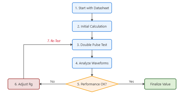
Step 1: Start with the Datasheet
The IGBT datasheet provides a recommended Rg value. This is your safest starting point. It’s typically specified for a particular set of test conditions (DC link voltage, current, temperature). Understand that this value is a compromise optimized by the manufacturer, like Infineon or Mitsubishi, for general use. Your specific application may require adjustments.
Step 2: Calculate the Initial Range
You can estimate the required Rg based on the desired switching time and the driver’s capability. For turn-on, the gate current needs to charge the input capacitance. A simplified view is:
Rg_total = (V_driver_on - V_plateau) / I_gate_avg
Where Rg_total = Rg_external + RGint. However, this is a rough approximation. A more practical approach is to use the datasheet value as the center of your test range and select values ±50% to evaluate.
Step 3: Laboratory Verification (The Double Pulse Test)
This is the most critical step. A double pulse test allows you to observe the IGBT’s switching behavior under controlled, real-world conditions without destroying it. You need a suitable DC power supply, a load inductor, a gate driver board, and a high-speed oscilloscope with appropriate voltage and current probes.
What to measure:
- Turn-on: Observe the collector current (Ic) rise time and the collector-emitter voltage (Vce) fall time. Look for any ringing on the gate-emitter voltage (Vge).
- Turn-off: This is where the most critical events happen. Carefully measure the peak Vce overshoot. It must remain well below the device’s Vces rating, with a safety margin (typically 15-20%). Also, check for Vge ringing.
- Switching Energy (Eon & Eoff): Use the oscilloscope’s math functions to integrate the product of Vce and Ic during the switching transitions to quantify losses.
Step 4: Fine-Tuning for Optimization
Analyze the waveforms from the double pulse test and adjust Rg accordingly:
- If Vce overshoot is too high: Increase the turn-off gate resistor (Rg_off).
- If switching losses are too high and overshoot is low: Cautiously decrease Rg_on and/or Rg_off, re-testing at each step to monitor the overshoot.
- If Vge shows significant ringing: Increase Rg_on and Rg_off. Check your layout for long traces or ground loops. Ensure the resistor is placed as close to the IGBT gate pin as possible.
Common Pitfalls and Troubleshooting
Even with a structured approach, issues can arise. Here are some common problems and their solutions:
- Problem: Excessive Voltage Overshoot (Vce peak).
Solution: The primary fix is to increase Rg_off to slow down the current fall time (dI/dt). If that overly increases switching losses, the next step is to minimize the power loop stray inductance through better busbar/PCB layout. A properly sized snubber circuit can also clamp the voltage. - Problem: Gate Voltage Ringing/Oscillation.
Solution: Increase Rg (both on and off). This adds damping to the resonant LC circuit of the gate loop. Ensure the gate resistor is placed physically as close as possible to the IGBT module’s gate and emitter/Kelvin-emitter pins. - Problem: Parasitic Turn-On (Miller Effect).
Solution: In a half-bridge, the fast-rising dV/dt across the low-side IGBT (as the high-side turns on) can induce a current through the Miller capacitance (Cgc), charging the gate. If the gate voltage rises above the threshold, it causes a momentary, destructive shoot-through. Solutions include using a strong Negative Gate Voltage during the off-state, or implementing an active Miller Clamp in the gate driver. Using a smaller Rg_off value than Rg_on also helps by providing a lower impedance path to ground.
Conclusion: Rg Selection is a System-Level Design Choice
The gate resistor is not a component to be selected in isolation. It is a critical tuning parameter that sits at the intersection of device physics, circuit layout, and application requirements. A successful design requires moving beyond the datasheet and embracing a system-level approach. By carefully balancing switching speed against voltage overshoot, EMI, and stability through methodical testing and validation, engineers can unlock the full potential of their power converters.
This optimization process ensures not only high efficiency but also the long-term reliability and robustness of the entire system. For expert assistance in selecting the right high-performance IGBT module for your application, such as the versatile FS450R17KE3, and for support in optimizing your gate drive circuit, contact the specialists at SLW-ELE.COM for tailored solutions.