The transition from Silicon IGBTs to Silicon Carbide (SiC) MOSFETs has fundamentally shifted power stage design. One of the most persistent questions in this transition is the necessity of negative gate voltage for turn-off. While traditional wisdom and early SiC generations dictated a bipolar drive (e.g., -5V/+15V) to prevent parasitic turn-on, the industry is increasingly moving toward simplified, single-supply (0V/+15V) architectures.
This article provides a rigorous engineering analysis of 0V turn-off feasibility. We move beyond ideal conditions to examine worst-case scenarios, the impact of threshold voltage drift, and the specific “red lines” where negative bias remains mandatory.
 Bipolar Supply vs. Single Supply with Active Miller Clamp
The Physics of Parasitic Turn-On: A Reality Check
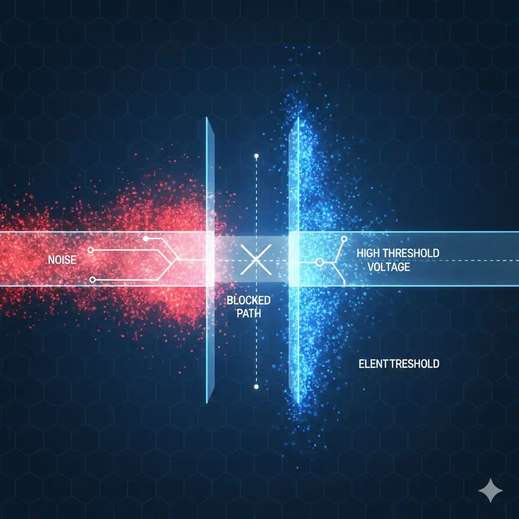
The primary argument for negative turn-off voltage is immunity against the Miller effect. As detailed in fundamental studies by Texas Instruments, when a MOSFET is off, and its complementary switch turns on, the high rate of change of voltage (dV/dt) across the drain-source terminals pumps current through the Miller capacitance (Cgd) into the gate loop.
The Mathematical Approximation
Engineers often use a capacitive divider model to estimate the induced gate voltage peak (Vgs,induced):
Vgs,induced ≈ Vbus × [ Cgd / ( Cgd + Cgs ) ]
Engineering Note: This formula serves as a first-order approximation for design intuition. In reality, Cgd is highly non-linear (changing drastically with Vds), and the peak voltage is further amplified by the parasitic inductance (Ls) in the source path and the gate loop layout. Therefore, the calculated safety margin must be treated conservatively.
To understand how these parasitic elements differ between device types, refer to this comparison of SiC vs. IGBT technologies.
Feasibility Factor 1: The Threshold Voltage (Vgs(th)) Dilemma
The viability of 0V turn-off hinges entirely on the device’s threshold voltage. However, relying on the “Typical” value found in datasheets is a common design error.
Worst-Case Design (Min/Max and Temperature)
For a robust design, engineers must consider the Vgs(th),min—the lowest possible threshold voltage allowed by the manufacturing process. Furthermore, Vgs(th) has a negative temperature coefficient. As the junction temperature (Tj) rises to 150°C or 175°C, the threshold voltage drops significantly.
- Gen 1 SiC: Often had Vgs(th) dropping below 1.5V at high temperatures, making 0V turn-off extremely risky.
- Modern Trench SiC (Gen 3+): Vendors like Infineon (CoolSiC™), Rohm (Gen 4), and Wolfspeed have optimized their trench structures to maintain higher threshold voltages (typically >4V at room temperature) and tighter process controls.
This structural evolution is what makes unipolar driving feasible today, provided that the worst-case, high-temperature Vgs(th) still offers sufficient headroom above the induced Miller voltage.
Feasibility Factor 2: Capacitance Ratios
The “Miller Ratio” (Cgd / Cgs) is critical. A lower ratio means less voltage is coupled to the gate during switching transients. Modern SiC MOSFET designs inherently optimize this ratio to be lower than their Silicon predecessors. By increasing the internal Cgs, manufacturers effectively create an internal capacitive clamp that attenuates noise.
The “Red Line”: When is 0V Turn-Off NOT Feasible?
While 0V turn-off is attractive for reducing BOM cost and complexity, it is not a universal solution. The following conditions represent the “failure boundary” where a negative bias (e.g., -3V or -5V) is strongly recommended or mandatory:
| Parameter | Condition for 0V Feasibility | Risk Zone (Negative Bias Required) |
|---|---|---|
| Package Type | 4-pin (Kelvin Source) or Low-Inductance Modules | 3-pin TO-247 (Common Source Inductance > 5nH) |
| Switching Speed (dV/dt) | Moderate (< 50 V/ns) | Extreme (> 80-100 V/ns) |
| Noise Environment | Tightly optimized PCB layout | High EMI, long gate traces |
For high-power modules where inductance is unavoidable, reviewing robust gate drive design principles is essential to prevent shoot-through.
Design Strategy: The Active Miller Clamp
If your design sits on the boundary—where 0V is desired for simplicity but dV/dt is high—the Active Miller Clamp is the industry-standard compromise.
Instead of a continuous negative rail, the gate driver IC monitors the gate voltage during the off-state. When the voltage drops below a set level (e.g., 2V), an internal MOSFET connects the gate directly to the Kelvin source/ground with a very low impedance path. This bypasses the external turn-off resistor (Rg,off), effectively “locking” the gate at 0V during the switching transient.
This technique allows for safe operation without the cost and space penalty of an isolated negative supply rail. This simplification is critical, as Analog Devices highlights that managing isolated bias power is often the most complex aspect of high-voltage system design. For detailed implementation guidelines, STMicroelectronics provides specific data on unipolar driving limits.
Application Suitability
Recommended for 0V Turn-Off:
- Solar String Inverters & UPS: Cost-sensitive, high-efficiency designs where Kelvin-source discrete devices are used.
- Light EV Chargers (OBC): Where space is at a premium and 650V/1200V CoolSiC or similar devices are employed.
Recommended for Negative Bias:
- Traction Inverters: Reliability is the absolute priority. The cost of a negative rail is negligible compared to the risk of inverter failure.
- High-Current Power Modules: Large modules often have higher internal gate loop inductance, making them more prone to ringing. For insights into high-power charging architectures, see our guide on 800V charging platforms.
Conclusion: A Calculated Engineering Decision
Eliminating the negative turn-off voltage is a legitimate design optimization, not just a cost-cutting measure. However, it requires a holistic view of the system. It is feasible only when using modern SiC devices with high Vgs(th) stability, low-inductance packaging (Kelvin source), and rigorous layout practices.
Engineers must validate the design not just at room temperature, but across the full operational thermal envelope, ensuring that the worst-case induced voltage never breaches the minimum threshold voltage. As SiC technology matures, 0V turn-off is becoming the standard for compact power conversion, but it demands a higher level of design precision.
For more deep dives into power semiconductor reliability and selection, explore the engineering resources at Shunlongwei Electronics.