In the rapidly evolving landscape of power electronics, Gallium Nitride (GaN) has emerged as a transformative material, pushing the boundaries of efficiency and power density far beyond the limits of traditional silicon-based MOSFETs. While silicon has been the industry workhorse for decades, the exponential energy demands of AI data centers, EV charging infrastructure, and renewable energy systems have paved the way for wide bandgap (WBG) semiconductors.
However, transitioning from Silicon (Si) to GaN is not a simple “drop-in” replacement. The very characteristics that make GaN superior—ultra-fast switching speeds and extremely low parasitic capacitances—also introduce significant design challenges. To achieve a successful design, engineers must fundamentally shift their mindset regarding layout, gate driving, and measurement techniques. This article explores the five critical areas every designer must master when working with GaN power transistors.

1. Understanding Device Limits and Material Benefits
The primary reason designers turn to GaN is its superior figure of merit. Unlike silicon superjunction MOSFETs, GaN is a lateral device with zero minority carrier-induced reverse recovery. In practical terms, this means the Qrr (reverse recovery charge) is effectively zero, dictated only by the device’s capacitance. This characteristic allows for much higher switching frequencies without the prohibitive switching losses seen in silicon.
When comparing GaN to Silicon Carbide (SiC) and Silicon (Si), several key parameters stand out, particularly at elevated temperatures:
- RDS(on) Temperature Coefficient: While GaN offers exceptionally low on-resistance, it typically exhibits a stronger temperature coefficient than SiC. At 125°C, the RDS(on) of a GaN device may increase more significantly than its silicon counterparts, requiring careful thermal sizing.
- Pulse Current Handling: GaN devices often have lower pulse current ratings relative to their continuous current ratings compared to massive silicon dies. Designers must pay close attention to peak current limits, especially at maximum operating temperatures, to avoid thermal runaway.
- Gate Charge (Qg): GaN features extremely low gate charge due to its low threshold voltage and minimal capacitance. This enables the fast switching speeds (dv/dt) that define the technology but requires precise gate control.
Deep Dive: For a detailed technical comparison between these technologies, engineers can refer to our in-depth analysis on Si vs SiC vs GaN switching speeds and power losses.
2. Optimizing the Gate Drive Circuit
The gate drive is the “brain” of the power switch, and with GaN, it requires a specialized approach. Because GaN switches so quickly—often with slew rates exceeding 50 to 100 V/ns—the gate drive circuit must be robust enough to prevent accidental turn-on caused by high dv/dt transients (Miller turn-on).
Steady-State and Transient Current
One common mistake in GaN design is providing insufficient drive current. To fully turn on a Gate Injection Transistor (GIT) type GaN device, the driver must supply a specific steady-state current (Iss) through a series resistor (Rss). Without adequate current, the device may not stay fully enhanced, leading to increased conduction losses. Conversely, during the initial turn-on phase, the driver must “overdrive” the gate to quickly charge the device’s internal capacitance.
Safe Turn-Off Strategies
For high-power applications, the safest way to turn off a GaN transistor is to use a negative gate voltage (e.g., -3V). This provides a critical safety margin against the “Miller effect,” where the rapid rise of the drain-source voltage couples through the gate-drain capacitance (Cgd), potentially pulling the gate voltage back above the threshold.
Designers can find further practical implementation strategies in our guide on robust gate drive design for power semiconductors.
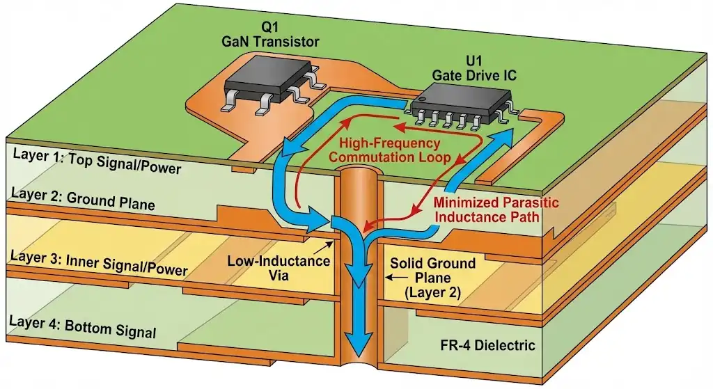
3. Minimizing Inductance in the Commutation Loop
In high-speed switching, PCB layout is not just a physical arrangement; it is an active electrical component. The “commutation loop”—the path that current takes during the transition between the high-side and low-side switches—is the most critical area for parasitic control.
At the speeds GaN operates, even a few nanohenries (nH) of PCB trace inductance can cause massive voltage spikes (V = L × di/dt) and ringing. To mitigate this, designers should utilize a vertical power loop layout. By placing the return path (ground plane) directly underneath the signal path on the next PCB layer, the magnetic fields generated by the current flow cancel out, significantly reducing the loop inductance.
For a deep dive into advanced layout techniques, major manufacturers provide extensive documentation. For example, Texas Instruments offers detailed GaN driver schematic and layout recommendations that illustrate these vertical loop concepts.
Furthermore, using a return-plane under the gate drive circuit provides essential shielding and a low-impedance return path, protecting sensitive control signals from the high-power switching noise. This principle is further explored in our resource on mastering GaN layout and signal integrity.
4. Precision Measurements: Beyond the 100 MHz Scope
Measuring GaN circuits is notoriously difficult. Standard probing techniques often introduce more noise than the signal being measured. If you observe 800 MHz or 900 MHz oscillations on your oscilloscope, it is often not the circuit ringing—it is your probe acting as an antenna.
The Equipment Barrier
A standard 100 MHz or 200 MHz oscilloscope is “barely adequate” for GaN. To accurately capture gate ringing and fast transitions, a minimum bandwidth of 500 MHz is required, though 1 GHz is strongly recommended. The EPC “GaN First Time Right” design guide emphasizes the importance of measurement bandwidth in validating high-speed designs.
Isolated Probes and CMTI
The high-side gate-source voltage (VGS) measurement is the ultimate challenge. Because the high-side source is “floating” and switching at high dv/dt relative to ground, standard differential probes often lack the necessary Common Mode Transient Immunity (CMTI). Optically isolated probes are the gold standard here, providing the necessary galvanic isolation to validate that gate signals are operating as expected without introducing ground loops.

5. Validation via Double-Pulse Testing
Before applying full power to a new GaN design, it is vital to validate the switching behavior using the Double-Pulse Test (DPT) technique. This allows the engineer to exercise the transistor through its entire range of voltage and current in a controlled manner without the risks associated with continuous operation.
The DPT works by applying two distinct pulses to the low-side switch in a half-bridge configuration while the high-side switch acts as a freewheeling diode:
- Pulse 1: Ramps up the current in an inductive load to a specific target level.
- Turn-off: Evaluates the turn-off characteristics and voltage overshoot at a specific current.
- Pulse 2: Measures the turn-on behavior and reverse recovery effects (or lack thereof in GaN) of the system.
Starting the DPT with a low bus voltage (e.g., 10V or 20V) ensures that if there is a layout or timing error, the energy involved is too low to cause catastrophic damage. For industry-standard testing protocols, the JEDEC JC-70 committee has established guidelines specifically for wide bandgap power semiconductor characterization.
Thermal Management and PCB Integration
Finally, the electrical and thermal paths must be optimized independently. Top-side cooled GaN packages are increasingly popular because they allow the heat to be dissipated directly into a heatsink without forcing the thermal energy through the PCB dielectric. This frees up the backside of the PCB for a solid ground plane, which improves EMI shielding and power density.
For comprehensive guidelines on managing heat in high-density designs, Infineon’s PCB design guidelines for GaN power transistors offer excellent engineering insights into optimizing stack-up and thermal vias.
Summary of GaN Design Parameters
| Parameter | GaN (600V/650V) | Silicon Superjunction | Engineering Significance |
|---|---|---|---|
| Qrr (Reverse Recovery) | Zero (Capacitive only) | Very High | Enables high-frequency switching and significantly reduces EMI. |
| Qg (Gate Charge) | Very Low | High | Reduces driving losses but requires fast, precise drivers. |
| Switching Speed (dv/dt) | 100+ V/ns | Limited | Requires precision vertical-loop layout to minimize parasitic inductance. |
In conclusion, GaN technology offers a path to unprecedented efficiency, but it demands engineering excellence. By focusing on gate drive integrity, minimizing loop inductance, and using advanced measurement techniques like optically isolated probes and double-pulse testing, designers can successfully harness the power of Gallium Nitride for the next generation of power conversion.