The 1200 V CoolSiC™ MOSFET Advantage in Three-Phase Power Conversion
In the rapidly evolving landscape of power electronics, the transition from silicon (Si) to Wide Bandgap (WBG) materials is no longer a futuristic concept—it is an industrial standard. As global demand for high-efficiency energy conversion grows, particularly in electric vehicle (EV) charging, solar inverters, and industrial servo drives, engineers are hitting the physical limits of traditional silicon IGBTs.
The introduction of 1200 V Silicon Carbide (SiC) MOSFETs, specifically the trench-gate based CoolSiC™ technology, has fundamentally altered the design equation for three-phase power systems. By addressing the inherent switching losses of bipolar devices and simplifying gate drive complexity, these components allow engineers to achieve system efficiencies exceeding 99%.
This article analyzes the technical superiority of 1200 V CoolSiC™ MOSFETs over standard silicon solutions, focusing on the physics of switching losses, the benefits of high threshold voltage (Vgs,th) in gate driver design, and the system-level impact on topology selection.
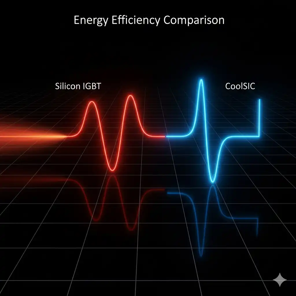 Figure 1: Conceptual comparison of switching waveforms. Note the elimination of tail current in the SiC device (right) compared to the Si IGBT (left).
1. The Physics of Loss: Why Silicon IGBTs Hit a Wall
To understand the advantage of SiC, we must first revisit the limitations of the Insulated Gate Bipolar Transistor (IGBT). For decades, the IGBT has been the workhorse of high-voltage power conversion. However, it is a bipolar device, meaning its conduction relies on the injection of minority carriers (holes) into the drift region to modulate conductivity.
While this modulation lowers on-state resistance, it creates a significant penalty during switching. When the IGBT turns off, these stored minority carriers must be swept out or recombine. This process is not instantaneous. It results in a phenomenon known as tail current—a lingering current flow that continues even after the gate voltage has dropped. Because this current exists while the voltage across the device (Vce) is rising, it generates substantial switching energy loss (Eoff).
For a deeper dive into the fundamental characteristics and historical applications of these devices, you can review our guide on IGBT basic knowledge and structure.
The Unipolar Advantage
In contrast, the CoolSiC™ MOSFET is a unipolar device. Current is carried essentially by majority carriers (electrons). When the device turns off, there are no minority carriers to recombine. Consequently, the “tail current” is effectively eliminated. The turn-off event is governed almost entirely by the charging of the parasitic capacitances (Coss).
This fundamental physical difference results in dynamic losses that are roughly an order of magnitude lower than those of a comparable 1200 V silicon IGBT. For engineers, this unlocks two critical design paths:
- Higher Switching Frequencies: Systems can operate at 20–50 kHz or higher without thermal runaway, drastically reducing the size of passive components (magnetics and capacitors).
- Lower Thermal Load: At standard frequencies, the cooler operation allows for smaller heatsinks and higher power density.
2. Solving the “Miller” Challenge: The High Threshold Voltage (Vgs,th)
One of the most persistent challenges in driving SiC MOSFETs is preventing Parasitic Turn-On (PTO). This phenomenon occurs in bridge configurations (like the three-phase inverter) during high-speed switching events.
The Mechanism of Parasitic Turn-On
When the high-side switch turns on, the voltage at the switch node rises rapidly (high dV/dt). This rapid voltage change acts across the Miller capacitance (Cgd) of the low-side switch (which is supposed to be off). A displacement current flows through Cgd, into the gate loop, and through the gate resistor (Rg). If the resulting voltage drop across the gate resistor exceeds the device’s threshold voltage (Vgs,th), the low-side device momentarily conducts. This causes a shoot-through event, leading to immediate efficiency loss and potential device failure.
The 4.5 V Solution
First-generation SiC planar devices often featured low threshold voltages (sometimes as low as 2 V). To prevent PTO, designers had to use complex gate drivers that applied a negative bias (e.g., -5 V) during the off-state to hold the gate firmly below the threshold.
The 1200 V CoolSiC™ trench technology addresses this at the chip level. By optimizing the trench gate structure, Infineon achieved a typical threshold voltage of approximately 4.5 V. This is significantly higher than many competitors.
Why does this matter? A higher Vgs,th provides a natural immunity to the Miller effect. The gate voltage induced by high dV/dt transients is far less likely to breach the 4.5 V limit. This allows engineers to implement a 0 V turn-off gate drive strategy.
Benefits of 0 V Turn-Off:
- Simpler Circuitry: No need for negative voltage rails or dual-output power supplies for the gate driver.
- Reduced Cost: Standard, low-cost single-supply gate driver ICs can be used.
- PCB Layout: Fewer components mean less board space and fewer traces to route, reducing parasitic inductance.
 Figure 2: The high threshold voltage of CoolSiC™ enables simplified unipolar driving schemes (Right), eliminating the need for negative supply rails required by standard SiC devices (Left).
3. System Topology: 1200 V Capability in 3-Phase Applications
The voltage rating of the semiconductor dictates the available circuit topologies. In industrial grids (400 V AC) or EV charging infrastructure (800 V DC bus), the blocking voltage requirements are stringent.
Simplifying the Inverter
Traditionally, using 650 V silicon devices for these high-voltage applications required 3-level topologies (such as Neutral Point Clamped – NPC). While 3-level inverters offer good harmonic performance, they are complex. They require more switches (often 12 per phase leg instead of 6), more gate drivers, and intricate modulation algorithms.
With 1200 V CoolSiC™ MOSFETs, engineers can revert to the classical 2-level B6 topology (standard three-phase bridge) even for 800 V DC bus applications. The 1200 V rating provides ample safety margin against voltage overshoots caused by stray inductance.
This substitution offers a massive “complexity reduction” dividend:
- Component Count: Reduced by up to 50% compared to 3-level silicon solutions.
- Reliability: Fewer components statistically reduce the failure rate (FIT).
- Efficiency: Despite the simpler topology, the superior switching performance of SiC allows the 2-level inverter to match or exceed the efficiency of a complex 3-level silicon inverter.
For maintenance engineers transitioning from IGBTs, it is crucial to understand that while the topology looks familiar, the diagnostic approach changes. You can refer to our practical field guide on testing power modules, keeping in mind that SiC body diodes behave differently than IGBT freewheeling diodes.
4. Real-World Application: The Bidirectional Charger
A prime example of this technology in action is the bidirectional On-Board Charger (OBC) for electric vehicles. These systems must convert AC grid power to DC for the battery, and conversely, convert DC back to AC for Vehicle-to-Grid (V2G) services.
 Figure 3: Modern electric vehicle connected to a bidirectional DC fast charger using SiC technology.
In a standard silicon-based LLC resonant converter, the switching losses at light loads significantly degrade efficiency. Furthermore, the reverse recovery charge (Qrr) of the internal body diode in silicon MOSFETs is often too high for reliable hard-switching operation in the totem-pole PFC stage.
CoolSiC™ MOSFETs excel here due to their low Qrr. In a Totem-Pole PFC stage utilizing 1200 V CoolSiC™, designers can achieve:
- Power Density: > 3 kW/liter.
- Peak Efficiency: > 99%.
- Thermal Management: Reduced cooling requirements allow for fully sealed, liquid-cooled modules.
This capability effectively replaces the complex multi-stage silicon designs with leaner, cooler, and more reliable SiC implementations.
5. Design Considerations and Best Practices
While the benefits are clear, replacing IGBTs with SiC MOSFETs is not a simple “drop-in” replacement. The high switching speed (dV/dt > 50 V/ns) requires careful attention to PCB layout.
Stray Inductance is the Enemy:
Because di/dt is extremely high, even a few nanohenries of stray inductance in the commutation loop can cause massive voltage spikes (V = L × di/dt). Engineers must use low-inductance packages (such as 4-pin TO-247 with a Kelvin source) and optimize the DC link capacitor layout to minimize the loop area.
Gate Resistor Selection:
Unlike IGBTs where Rg is used to slow down switching to prevent EMI, SiC requires a balance. If Rg is too high, you lose the switching loss advantage. If it is too low, voltage overshoot may exceed the breakdown rating. The high Vgs,th of CoolSiC™ offers a wider safe operating area (SOA) for tuning these resistors without risking parasitic turn-on.
For more insights into common thermal and electrical issues in power switching, see our discussion on common problems in power device applications, which, while focused on IGBTs, offers relevant thermal management principles.
Conclusion
The 1200 V CoolSiC™ MOSFET represents more than just a material upgrade; it is a systemic enabler. By combining the physics of wide bandgap materials with a robust trench-gate design, it eliminates the “tail current” losses that have plagued silicon IGBTs for decades.
For the design engineer, the specific high-threshold voltage characteristic of CoolSiC™ is perhaps its most practical feature. It allows for the high-performance switching of SiC without the penalty of complex, bipolar gate drive circuits. Whether in servo drives, solar inverters, or the next generation of EV chargers, the ability to drive a 1200 V switch with a simple 0 V turn-off signal facilitates a leap forward in power density and reliability.
As the industry pushes toward higher voltages and compact form factors, mastering the application of these devices will be the defining skill for power electronics engineers in the coming decade.
References & Further Reading:
Content in This Series

Mitigating Parasitic Turn-On (PTO) in SiC MOSFETs: The Critical Role of Miller Capacitance and Threshold Voltage Optimization
