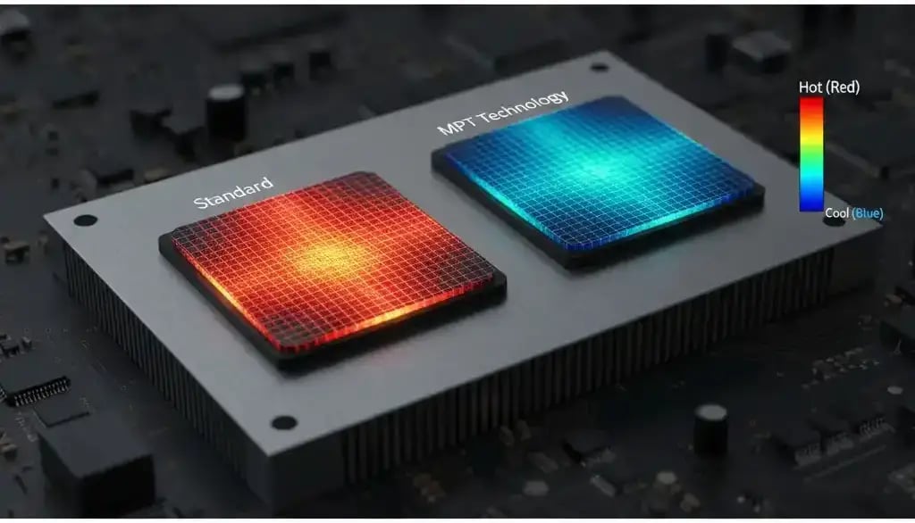
In the relentless pursuit of power density and efficiency in industrial electronics, the evolution of the Insulated Gate Bipolar Transistor (IGBT) has reached a critical inflection point. For decades, the trade-off between conduction losses (VCE(sat)) and short-circuit ruggedness defined the boundaries of silicon power device design. However, the introduction of the Micro-Pattern Trench (MPT) cell structure in modern 7th-generation IGBTs (such as the IGBT7) marks a fundamental shift in how engineers manage these competing parameters.
This article provides a comprehensive engineering analysis of the MPT architecture. We will move beyond the datasheet values to explore the semiconductor physics governing this design, focusing on how sub-micron mesa structures and optimized trench geometries enable the suppression of static losses while maintaining critical robustness for 1200 V industrial drive applications.
For a broader understanding of how these modules fit into high-efficiency systems, you can refer to our guide on IGBT modules as the backbone of power systems.
1. The Architectural Shift: From Square Cells to MPT Strips
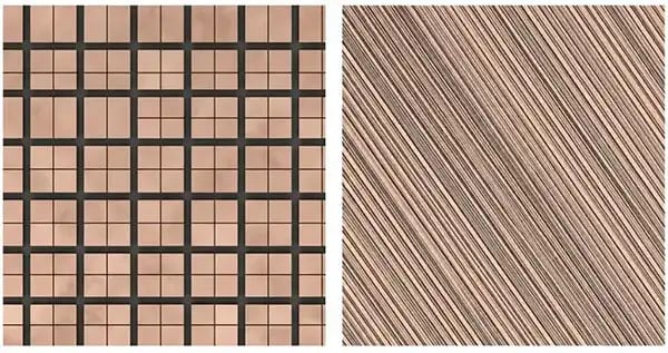
To understand the significance of Micro-Pattern Trenches, we must first revisit the limitations of the previous industry standard: the trench-gate field-stop structure (often exemplified by IGBT4). Traditional designs typically utilized a square or hexagonal trench cell layout. While effective, this geometry imposed limits on the channel density and the ability to manipulate the carrier concentration at the emitter side of the drift region.
The MPT structure abandons the cellular layout in favor of a highly configurable stripe pattern. This is not merely a cosmetic change; it is a functional reconfiguration of the active silicon area. By adopting a parallel stripe layout, chip designers can precisely control the ratio of “active” trenches (connected to the gate) to “inactive” or dummy trenches (connected to the emitter or floating).

The most defining feature of MPT, however, is the drastic reduction in mesa width. The mesa—the silicon region between two adjacent trenches—has been scaled down to the sub-micron level. This dimensional scaling is the primary driver behind the enhanced electrical performance of 7th-generation devices.
2. Physics of Loss Reduction: The Carrier Storage Effect
The primary goal of the MPT structure is to reduce the on-state voltage drop, VCE(sat), without increasing the turn-off losses (Eoff). This is achieved by maximizing the Carrier Storage Effect.
Conductivity Modulation and Plasma Distribution
In a bipolar device like an IGBT, current conduction is facilitated by the injection of holes from the p-collector and electrons from the n-emitter (channel). The concentration of these electron-hole pairs (plasma) in the n-drift region determines the conductivity. Higher plasma concentration results in lower resistance.
In standard trench structures, holes injected from the collector tend to drain out quickly through the emitter contact. This results in a lower carrier concentration near the top (emitter side) of the chip, leading to a higher VCE(sat).
The Barrier Effect of Sub-Micron Mesas
The MPT structure utilizes its sub-micron mesa width to create a “barrier” to hole extraction. Because the mesa is so narrow, the path for holes to reach the emitter contact is restricted. This structural bottleneck forces an accumulation of holes at the cathode side of the drift layer. Consequently, to maintain charge neutrality, the electron concentration also increases.
This phenomenon drastically enhances the carrier concentration profile, making it nearly flat across the drift region. The result is a device that behaves closer to an ideal diode in conduction, exhibiting a significantly lower VCE(sat) compared to previous generations. For a 1200 V device, this improvement allows for a substantial reduction in static losses, which is critical for low-frequency drive applications.
For more on how these advancements specifically impact industrial drives, see our analysis on unlocking efficiency in industrial drives with IGBT7 technology.
3. The Trade-Off: Maintaining Short-Circuit Robustness
Historically, increasing the channel density and conductivity modulation to lower VCE(sat) came with a severe penalty: a massive increase in short-circuit current (ISC). If the short-circuit current is too high, the device can destroy itself thermally within microseconds, long before the gate driver’s protection circuit can intervene.
This is where the flexibility of the MPT design becomes crucial. If every stripe in the MPT structure were an active gate-controlled channel, the ISC would be uncontrollable. However, the MPT architecture allows engineers to implement intermittent active channels.
- Active Trenches: Connected to the gate potential, responsible for forming the inversion channel and conducting current.
- Inactive (Dummy) Trenches: Connected to the emitter potential. These do not conduct channel current but contribute to the charge storage effect and electric field distribution.

By adjusting the ratio of active to inactive trenches (e.g., k:1 ratio), designers can effectively “throttle” the saturation current. This allows the device to maintain a low VCE(sat) due to the high carrier density from the sub-micron mesas, while simultaneously limiting the short-circuit current to a safe level.
The 8 µs Requirement
For 1200 V industrial applications, the standard requirement for short-circuit withstand time (tSC) is typically 10 µs for previous generations. However, due to the higher power density and optimized thermal performance of MPT-based devices, they are often rated for 8 µs at a junction temperature of 175°C. While slightly lower than the legacy 10 µs, this is sufficient for modern, fast-acting gate drivers to detect desaturation and shut down the system safely.
Understanding desaturation detection is vital for implementing these devices. We recommend reading Why Does IGBT Desaturation Occur? to understand the protection mechanisms required.
4. Technical Comparison: MPT vs. Standard Trench
To visualize the engineering impact of the MPT structure, we compare it against the standard trench-gate field-stop technology typically found in 4th generation devices. The table below highlights the key parametric shifts.
| Parameter | Standard Trench (e.g., IGBT4) | Micro-Pattern Trench (MPT) (e.g., IGBT7) | Engineering Impact |
|---|---|---|---|
| Cell Structure | Square / Hexagonal Cells | Sub-micron Parallel Strips | MPT allows independent optimization of conduction and switching. |
| VCE(sat) | Baseline (Approx. 2.05V @ Nom) | Significantly Lower (Approx. 1.75V @ Nom) | Reduced conduction losses; higher efficiency in low-switching-frequency drives. |
| Carrier Profile | Gradient (Low near emitter) | Flat / Accumulation near emitter | Enhanced conductivity modulation (Carrier Storage Effect). |
| Short Circuit Time | 10 μs | 8 μs | Requires faster desaturation detection; trade-off for higher efficiency. |
| Junction Temp (Tvj,op) | 150°C | 175°C | Allows for higher overload capability and power density. |
5. Implementation Considerations for Engineers
Adopting MPT-based IGBTs is not a “drop-in” replacement in every scenario; it requires specific design considerations to maximize benefits while ensuring reliability.
Gate Driving and dv/dt Control
The MPT structure typically exhibits a higher gate capacitance due to the trench density, but the gate charge (Qg) characteristics are optimized. One specific characteristic of MPT devices is their controllability of voltage slope (dv/dt) via the gate resistor (Rg). Unlike some older technologies where dv/dt saturated quickly, MPT devices offer a wide controllable range.
This allows engineers to tune the Rg to balance switching losses against Electromagnetic Interference (EMI) and voltage overshoot. For applications involving long motor cables, managing the dv/dt is critical to preventing motor insulation failure and reflection voltage spikes.
Thermal Management and Heatsinking
Since the VCE(sat) is lower, the static heat generation is reduced. This is particularly beneficial in applications like General Purpose Drives (GPD), where the switching frequency is typically low (2 kHz – 8 kHz). In these scenarios, conduction losses dominate the thermal budget. The MPT structure allows engineers to either output more current with the same heatsink or shrink the cooling system for the same power rating.

Conclusion
The Micro-Pattern Trench (MPT) cell structure represents a sophisticated manipulation of semiconductor physics. By leveraging sub-micron geometries to enhance the carrier storage effect, engineers have successfully decoupled the rigid link between conduction efficiency and device ruggedness.
For the power electronics engineer, MPT technology offers a pathway to significantly higher system efficiency, particularly in variable frequency drives (VFDs) and servo systems. However, it necessitates a careful approach to protection circuits, specifically respecting the 8 µs short-circuit capability and optimizing gate resistance for EMI compliance. As 1200 V systems continue to evolve, the ability to control losses at the cellular level will remain a cornerstone of high-performance power conversion.
To explore more about ensuring robustness in inductive load applications, review our guide on Avalanche Energy and Ruggedness, which shares parallel concepts in device reliability.
