The advent of Silicon Carbide (SiC) technology has revolutionized power electronics, enabling power converters to operate at higher voltages, higher temperatures, and significantly faster switching frequencies compared to traditional Silicon (Si) IGBTs. However, this leap in performance brings specific engineering challenges. The most notorious among them is the Parasitic Turn-On (PTO) effect, a phenomenon that poses a significant threat to system reliability in bridge topologies.
For power electronics engineers, understanding the physics behind PTO is not merely academic—it is a prerequisite for designing robust, high-efficiency inverters and power supplies. This article delves into the physical mechanisms of the Miller effect, analyzes the mathematical relationships governing dv/dt immunity, and explores how modern device structures, such as those found in advanced electronic components like CoolSiC™, address these challenges through optimized capacitance ratios and elevated threshold voltages.
1. The Physics of Parasitic Turn-On (PTO)
Defining the Phenomenon
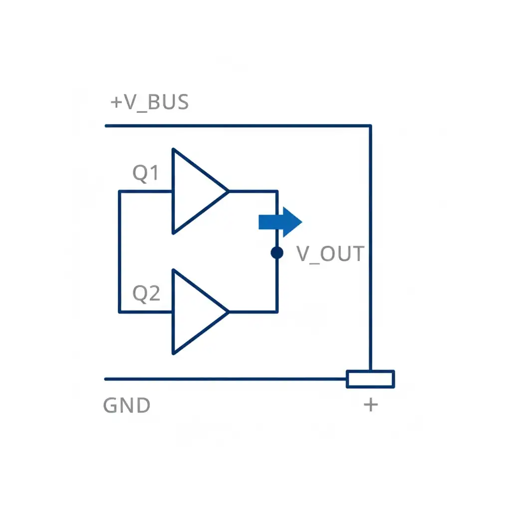
Parasitic Turn-On, often referred to as spurious turn-on, occurs in half-bridge or full-bridge configurations where two switches (high-side and low-side) are connected in series across a DC bus. The phenomenon typically affects the device that is intended to be in the “off” state (the victim) while the complementary device (the aggressor) switches on.
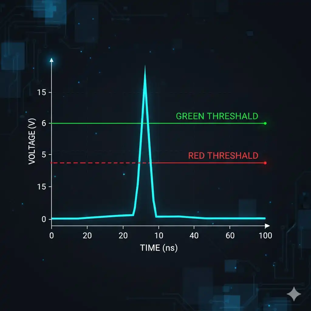
When the high-side switch turns on, the voltage across the low-side switch (Vds) rises rapidly from near zero to the full bus voltage. This rapid change in voltage over time, denoted as dv/dt, is the catalyst for PTO. In modern SiC applications, dv/dt rates can easily exceed 50 V/ns or even 100 V/ns. This high slew rate interacts with the intrinsic parasitic capacitances of the MOSFET, creating a dangerous feedback loop.
The Miller Effect and Displacement Current
The core of the problem lies in the Miller Capacitance, physically represented as the Gate-Drain capacitance (Cgd). Although Cgd is physically small compared to other internal capacitances, it acts as a bridge connecting the high-voltage drain to the sensitive gate terminal.
According to fundamental physics, a changing voltage across a capacitor generates a displacement current (idisplacement). The magnitude of this current is governed by the equation:
ig = Cgd × (dv/dt)
This displacement current flows from the drain, through the Miller capacitor, and into the gate node. From the gate node, it must find a path back to the source. It flows through the gate resistor (Rg,ext) and the internal gate driver impedance. This current flow creates a voltage drop across the total gate loop resistance, effectively lifting the potential of the gate relative to the source.
If this induced voltage spike (Vgs,induced) exceeds the device’s Gate Threshold Voltage (Vgs,th), the MOSFET—which should be strictly off—begins to conduct. This results in a momentary short circuit across the DC bus, known as shoot-through.
2. The Consequences of Shoot-Through
The implications of PTO are severe and multifaceted. Unlike a catastrophic short circuit that destroys a device instantly, PTO often manifests as a “silent killer” that degrades efficiency and reliability over time before causing total failure.
- Increased Switching Losses: Even partial conduction allows current to flow while the voltage is high. This V × I product results in significant energy dissipation, negating the efficiency gains expected from SiC technology.
- Thermal Stress: The additional heat generated by shoot-through events raises the junction temperature. As many parameters (including Vgs,th) are temperature-dependent, this can create a positive feedback loop leading to thermal runaway.
- Electromagnetic Interference (EMI): The current spikes associated with shoot-through generate high-frequency noise, complicating filter design and potentially violating EMC compliance standards.
To avoid these issues, engineers must carefully select semiconductor devices with robust intrinsic characteristics.
3. Critical Evaluation Metrics: The Capacitance Ratio
Evaluating a SiC MOSFET’s immunity to PTO requires looking beyond simple breakdown voltage or Rds(on). The dynamic relationship between the device’s parasitic capacitances is the primary determinant of its stability under high dv/dt conditions.
The Capacitance Divider
The gate terminal forms a capacitive voltage divider between the drain and the source. The induced voltage on the gate can be approximated (ignoring resistive damping for a worst-case static analysis) by the ratio of the Miller capacitance to the total input capacitance:
Vgs,induced ≈ Vbus × [ Cgd / (Cgd + Cgs) ]
Here, Cgs is the Gate-Source capacitance. To minimize the induced voltage, the ratio Cgd / Cgs must be kept as low as possible. A lower Miller capacitance (Cgd) reduces the injection of current, while a larger Source capacitance (Cgs) helps clamp the gate voltage by absorbing the charge.
Design Trade-offs
While increasing Cgs improves PTO immunity, it also slows down the switching speed and increases driving losses. Therefore, the most elegant solution is not to arbitrarily increase Cgs, but to minimize Cgd through advanced structural engineering of the MOSFET trench or planar architecture. For deeper insights into these mechanisms, refer to recent studies on Parasitic Turn-On mechanisms.
4. The Role of Threshold Voltage (Vgs,th)
The capacitance ratio defines the magnitude of the voltage spike, but the Threshold Voltage (Vgs,th) determines the safety margin. This is where significant differences exist among industry players.
In the SiC landscape, manufacturers have taken different approaches to Vgs,th:
| Parameter | Standard Planar SiC MOSFET | Optimized Trench SiC (e.g., CoolSiC™) |
|---|---|---|
| Typical Vgs,th | 2.0 V – 3.0 V | ~ 4.5 V |
| Temperature Drift | Decreases significantly at 150°C | Stable, remains high |
| Noise Margin | Low (High Risk) | High (Low Risk) |
As shown in the table, many standard SiC devices feature a threshold voltage around 2.5 V. While this allows for easy turn-on, it leaves a perilously thin margin for noise. In high-power applications where dv/dt noise is rampant, a 2.5 V threshold can be easily breached by a Miller-induced spike, especially at high operating temperatures where Vgs,th naturally decreases.
The CoolSiC™ Advantage
Advanced trench gate structures, such as those employed in Infineon’s CoolSiC™ technology, are designed to maintain a significantly higher threshold voltage, typically around 4.5 V. This design choice provides a robust buffer against PTO.
With a 4.5 V threshold, the device can tolerate a much higher induced gate voltage before conducting. This is particularly critical in harsh industrial environments involving motor drives or solar inverters, where ground bounce and EMI are common.
5. Simplifying Gate Drive Designs: 0 V Turn-Off
One of the most tangible benefits of using SiC MOSFETs with high Vgs,th and optimized capacitance ratios is the simplification of the gate driver circuit.
The Negative Voltage Burden
To prevent PTO in devices with low threshold voltages (e.g., 2.5 V), engineers are often forced to use a negative turn-off voltage (e.g., -5 V or -4 V). By biasing the gate negatively in the off-state, the designer artificially increases the voltage distance to the threshold. For example, if the gate is held at -5 V, a 7 V spike is required to reach a 2 V threshold.
However, implementing negative gate bias introduces complexity:
- Dual Supply Requirements: The power supply for the gate driver must provide both positive and negative rails (e.g., +15 V / -5 V), increasing the component count and cost.
- Gate Oxide Stress: Continuous negative bias can contribute to gate oxide drift (Vgs drift) over the lifetime of the device, potentially affecting long-term reliability. See more on reliability and failure modes.
The Unipolar Solution
Due to the optimized Miller ratio and the inherently high threshold voltage of 4.5 V, devices like CoolSiC™ can be safely driven with 0 V turn-off bias. This means a simple unipolar supply (e.g., 0 V to 15 V) is sufficient to drive the switch reliably, even under 800 V / 15 A / 150°C operating conditions. Detailed validation of this performance can be found in Infineon’s technical analysis on CoolSiC™ parasitic turn-on behavior.
This capability simplifies the PCB layout, reduces the bill of materials (BOM), and eliminates the need for complex charge pump circuits or specialized dual-output DC-DC converters for the gate driver.
6. Best Practices for Design and Layout
While selecting the right component is half the battle, the physical implementation on the Printed Circuit Board (PCB) is equally vital. Even the most robust SiC MOSFET can fail if the layout introduces excessive parasitic inductance.
Minimizing Gate Loop Inductance
The inductance in the source path (common source inductance) acts as negative feedback, but inductance in the gate loop can cause ringing. Engineers should minimize the trace length between the driver and the gate. Utilizing a Kelvin Source connection is highly recommended. The Kelvin Source separates the power current path from the gate drive signal reference, virtually eliminating the effect of common source inductance on the gate signal and preventing false triggering due to inductive voltage drops.
Active Miller Clamping
For applications pushing the limits of switching speed (extreme dv/dt), designers might still opt for an Active Miller Clamp. This technique involves a transistor in the gate driver that shorts the gate to the source or a negative rail during the off-state, providing a low-impedance path for the Miller current. However, with high-threshold devices, this adds complexity that may not be necessary for many standard applications.
Conclusion
The transition from Silicon to Silicon Carbide is driven by the demand for efficiency and power density. However, the high-speed nature of SiC introduces Parasitic Turn-On as a fundamental challenge that must be addressed at both the device and system levels.
The interaction between the Miller capacitance (Cgd), the switching speed (dv/dt), and the gate threshold voltage (Vgs,th) defines the immunity of a system to shoot-through failures. While circuit-level workarounds like negative gate bias exist, they add cost and complexity.
The superior approach is to select electronic components designed with these physics in mind. Technologies like CoolSiC™, characterized by low Cgd/Cgs ratios and high threshold voltages (4.5 V), offer “intrinsic” immunity. This allows engineers to adopt simplified 0 V turn-off driving schemes without compromising on safety or reliability. By understanding these parameters, designers can unlock the full potential of wide-bandgap technology, ensuring that their power converters are not only fast but also robust and durable for the long haul.