The Race for Efficiency: Modular Architectures in 150kW to 350kW BEV DC Fast Chargers
As the global adoption of Battery Electric Vehicles (BEVs) accelerates, range anxiety remains one of the primary hurdles for mainstream consumers. To mitigate this, the automotive and power electronics industries are aggressively pushing the boundaries of charging infrastructure. We are witnessing a rapid evolution from standard 50kW chargers to ultra-fast 150kW and 350kW charging modules. Delivering this massive amount of power safely, efficiently, and reliably requires highly sophisticated power electronics engineering.
At 350kW, a charging station can theoretically add hundreds of kilometers of range to an EV in under 15 minutes. However, processing 350kW of power from the AC grid to a high-voltage DC battery pack involves significant challenges in thermal management, power density, and electrical safety. This article provides a deep dive into the dominant DC fast charging topologies, explores the necessity of the modular approach, and dissects the critical power stages—specifically the Vienna Rectifier and the LLC Resonant Converter—that make these systems possible.
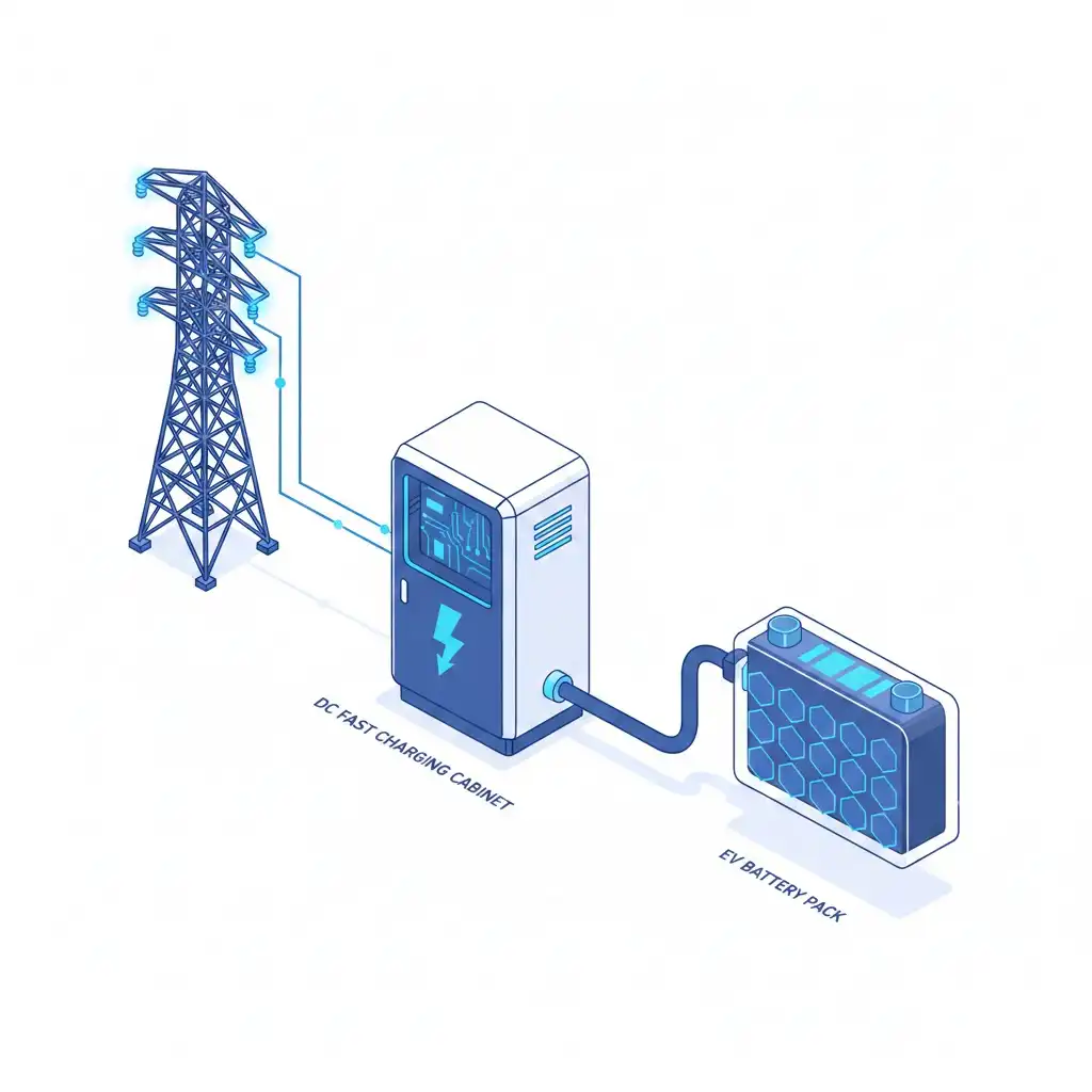 Figure 1: High-level overview of a typical DC Fast Charging Station connected to the grid and a Battery Electric Vehicle.
1. The Fundamental Architecture of High-Power DC Fast Chargers
A DC fast charger bypasses the vehicle’s onboard charger (OBC), delivering direct current directly to the high-voltage battery pack. To achieve this, the charging station must perform two primary power conversion steps: AC/DC rectification with Power Factor Correction (PFC), and isolated DC/DC conversion to regulate the voltage and current delivered to the battery.
When engineering a high-power DC fast charging topology, designers generally evaluate two primary architectural strategies:
Topology A: Variable DC Output Voltage
In this architecture, the front-end AC/DC PFC stage actively regulates its output voltage to directly match the changing voltage requirements of the EV battery pack during the charging cycle. The subsequent DC/DC stage primarily provides galvanic isolation and fine-tuned current regulation. While this reduces some complexity in the DC/DC stage, it forces the front-end PFC stage to operate over a very wide output voltage range, which can compromise the optimization of power factor and total harmonic distortion (THD) under certain grid conditions.
Topology B: Fixed DC Link with an Isolated DC/DC Stage
This is the dominant architecture in modern 150kW to 350kW charging modules. The front-end PFC stage maintains a highly stable, fixed intermediate DC link voltage (commonly 800V or 1000V DC). The downstream isolated DC/DC converter then steps this voltage down (or up) to match the EV battery. This decoupled approach allows both stages to be optimized independently. The PFC stage can be perfectly tuned for maximum grid compliance and a power factor near unity, while the DC/DC stage can be optimized for peak efficiency over the battery’s specific voltage range.
For more insights into handling these high voltage levels, engineers often refer to comprehensive design guides, such as Designing 150kW DC Fast Chargers with 1200V IGBTs.
2. The Modular Approach: Scaling to 350kW and Beyond
Building a monolithic 350kW power converter is generally impractical due to extreme thermal hotspots, massive magnetic components, and single-point-of-failure risks. Instead, the industry has universally adopted a modular approach.
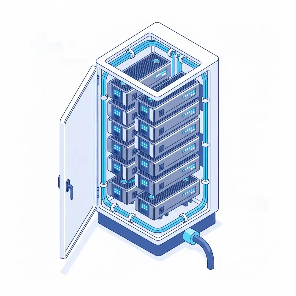
Figure 2: A modular architecture combining multiple smaller power modules in parallel to achieve a high total output power.
A 350kW charging station is typically composed of multiple smaller, highly integrated power sub-units, usually ranging from 15kW to 60kW each, connected in parallel. This architecture offers several profound engineering and operational advantages:
- High Scalability: Manufacturers can design a single standard module (e.g., a 30kW unit) and deploy it across various products. A 60kW charger uses two modules; a 350kW charger uses twelve.
- N+1 Redundancy and Reliability: In a monolithic design, a single semiconductor failure takes the entire station offline. In a modular design, if a single 30kW module fails, the master controller isolates it, and the station continues operating at 320kW. This is critical for infrastructure uptime.
- Interleaved Operation: By phase-shifting the switching cycles of parallel modules (interleaving), engineers can significantly reduce the input and output current ripple. Lower ripple means smaller filter capacitors are required and ensures that the EV battery cells are not stressed by high-frequency current fluctuations.
- Thermal Distribution: Dissipating the heat from several distributed modules is much easier than managing the concentrated thermal load of one massive converter block.
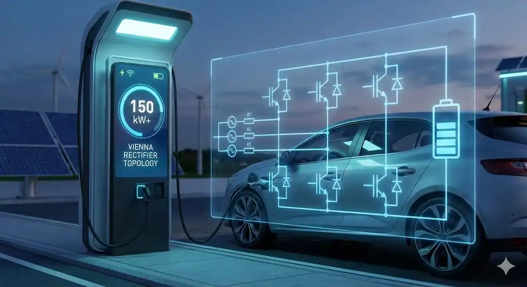
3. Deep Dive into the PFC Stage: The Vienna Rectifier
The first crucial stage in a DC fast charging topology is the active Power Factor Correction (PFC) rectifier. It must convert the three-phase AC grid voltage into a stable DC bus voltage while drawing sinusoidal current that is perfectly in phase with the grid voltage. For modules operating in the 15kW to 60kW range, the Vienna Rectifier has emerged as the industry standard.
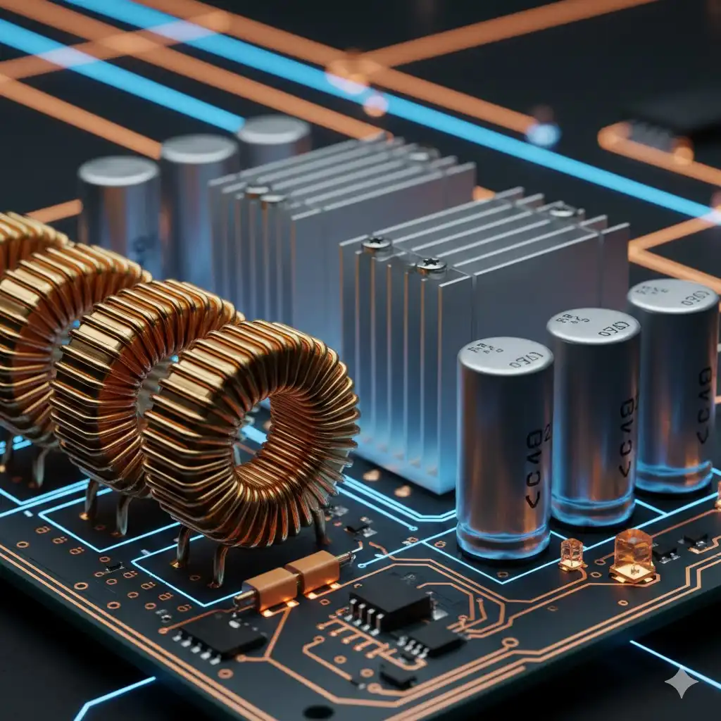
Figure 3: Schematic representation of a three-phase, three-level Vienna Rectifier.
Working Principle and Advantages
The Vienna Rectifier is a unidirectional, three-phase, three-level pulse-width modulation (PWM) rectifier. Unlike a standard two-level active front end, the Vienna Rectifier creates three distinct voltage levels at its input switch nodes. This is achieved by connecting the AC input phases to the center point of the DC output capacitors via bidirectional active switches.
The engineering advantages of the Vienna Rectifier for 350kW charging modules include:
- Reduced Voltage Stress on Semiconductors: In a system generating an 800V DC bus, a traditional two-level topology would subject the switching devices to the full 800V, requiring components rated for 1200V. The three-level Vienna topology divides the DC bus in half across the output capacitors. Consequently, the active switches only see half the DC bus voltage (e.g., 400V). This allows engineers to use highly efficient, lower-cost 600V or 650V rated silicon MOSFETs or fast IGBTs instead of expensive 1200V components.
- Exceptional Power Quality: Through advanced digital control loops, the Vienna Rectifier can easily achieve a Power Factor (PF) of 0.997 and a Total Harmonic Distortion (THD) of less than 3%. This prevents the charging station from polluting the local AC grid with reactive power and harmonic noise, which is strictly regulated by utility companies.
- Robustness Under Grid Faults: A significant advantage of the Vienna Rectifier is its operational robustness, particularly during a “phase loss” or “phase drop” event. If one of the three AC grid phases is temporarily lost due to a grid anomaly, the control system can detect the zero-crossing failure and instantly reconfigure the PWM strategy. The rectifier can often continue operating at reduced power on the remaining two phases, preventing a hard shutdown of the charging session.
For more theoretical background on this widely used active rectification method, you can review its historical development and variations on the Vienna Rectifier Wikipedia page.
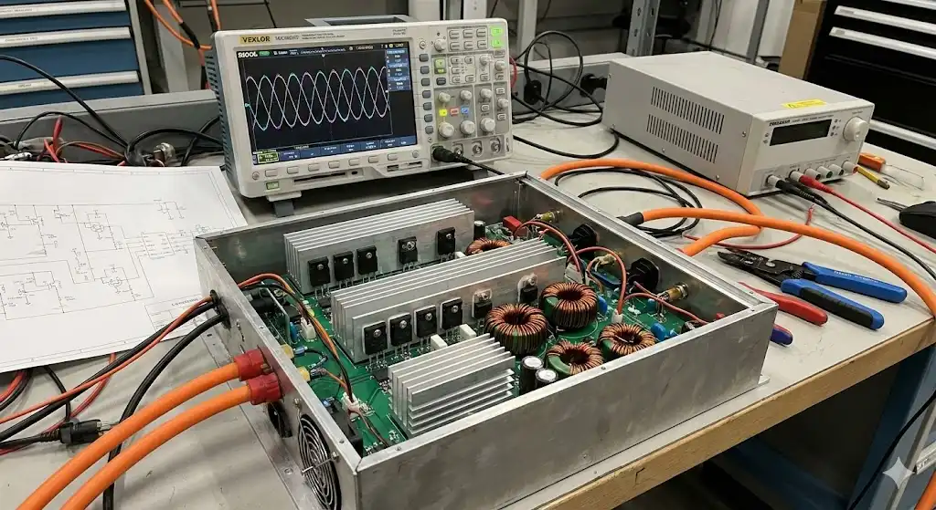
4. Achieving High Power Density: The LLC Resonant Converter
Following the PFC stage, the intermediate DC voltage (e.g., 800V) must be isolated and converted to the precise voltage required by the EV’s Battery Management System (BMS). This is typically handled by an isolated DC/DC converter. To meet the stringent power density and efficiency requirements of modern charging infrastructure, the Full-Bridge LLC Resonant Converter is the topology of choice.
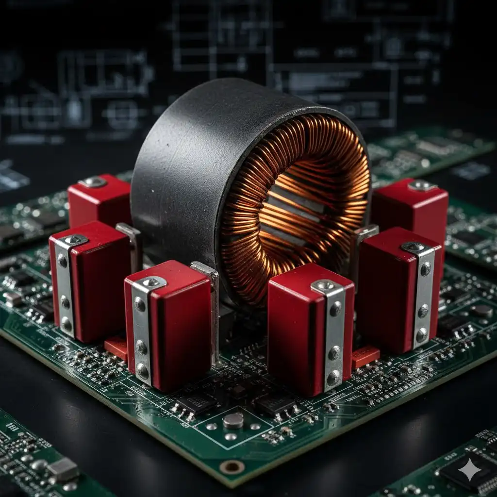
Figure 4: Topology of a Full-Bridge LLC Resonant DC/DC Converter showing the resonant tank.
The Mechanics of Resonance
Unlike traditional hard-switched PWM converters (where transistors turn on and off while high voltage and current are present across them), the LLC converter uses a resonant tank circuit to shape the voltage and current waveforms into sine waves. The resonant tank consists of three reactive components: a resonant inductor (Lr), a magnetizing inductor (Lm)—often integrated into the high-frequency transformer—and a resonant capacitor (Cr).
By modulating the switching frequency (fsw) of the primary-side transistors relative to the resonant frequency (fr) of the tank circuit, the controller regulates the output voltage. This frequency modulation approach allows the converter to achieve Zero Voltage Switching (ZVS).
The Importance of ZVS in High-Power Modules
Switching losses (Psw) occur because power semiconductor switches take a finite amount of time to transition between their ON and OFF states. During this brief overlap, both voltage (V) and current (I) are present across the device, resulting in power dissipation (P = V * I).
With Zero Voltage Switching, the LLC resonant tank creates a phase shift that causes the voltage across the primary transistors to drop to zero before the gate drive signal turns them on. Because the voltage is zero at the moment of switching, turn-on switching losses are effectively eliminated. Furthermore, the secondary-side rectification diodes often experience Zero Current Switching (ZCS), eliminating reverse recovery losses.
This drastic reduction in switching losses has a cascading effect on the entire design:
- Higher Efficiency: Efficiencies exceeding 98% are achievable in the DC/DC stage.
- Higher Switching Frequencies: Because switching losses are negligible, engineers can safely increase the switching frequency (e.g., from 50kHz to 150kHz or higher).
- Smaller Magnetics: A higher switching frequency means the high-frequency isolation transformer and filter inductors can be significantly smaller and lighter, drastically increasing the power density (kW/kg) of the 350kW charging module.
To understand the thermal implications of these switching parameters and how to manage the remaining heat, engineers must carefully consider junction-to-case thermal resistance, as discussed in our guide: Why Rth Matters: Unlocking IGBT Thermal Performance.
5. Silicon vs. Silicon Carbide (SiC): Striking the Right Balance
The efficiency and power density of both the Vienna Rectifier and the LLC converter are ultimately constrained by the physical limitations of the semiconductor materials used. The industry is currently in a transitional phase, balancing traditional Silicon (Si) Insulated-Gate Bipolar Transistors (IGBTs) and Super-Junction MOSFETs against wide-bandgap Silicon Carbide (SiC) devices.
The Silicon Carbide (SiC) Advantage
SiC MOSFETs possess physical properties that make them vastly superior to Silicon for high-power, high-voltage switching. They have a higher critical breakdown electric field, which allows for thinner drift layers and consequently a much lower ON-state resistance (RDS(on)). Furthermore, unlike IGBTs, SiC MOSFETs are unipolar devices; they do not suffer from minority carrier “tail current” during turn-off. This results in significantly lower turn-off switching energy (Eoff).
In the context of an EV charger, utilizing all-SiC modules allows the LLC converter to operate at frequencies well above 100kHz, shrinking the transformer size and pushing the module’s overall efficiency to the absolute maximum. For a deeper comparative analysis on this topic, see SiC vs. IGBT: The Technology Showdown Powering the Future of Electric Vehicles.
The Pragmatic Hybrid Approach
Despite their technical superiority, SiC MOSFETs remain significantly more expensive than traditional Silicon devices. In a highly competitive infrastructure market, the Bill of Materials (BOM) cost is a critical metric. Therefore, many engineers are adopting a pragmatic hybrid approach to optimize the cost-to-performance ratio.
In a typical 30kW charging module design:
- PFC Stage (Vienna Rectifier): The low-frequency line commutation switches (which operate at the 50Hz/60Hz grid frequency) can use inexpensive, low-conduction-loss Silicon IGBTs. The high-frequency switching positions in the Vienna rectifier can utilize Silicon Super-Junction MOSFETs combined with discrete SiC Schottky diodes. The SiC diodes eliminate reverse recovery currents, drastically improving efficiency without the cost of full SiC MOSFETs.
- DC/DC Stage (LLC): Depending on the target efficiency class (e.g., standard vs. premium), designers may use high-speed Silicon MOSFETs or opt for SiC MOSFETs if the space constraints demand ultra-high switching frequencies.
As SiC wafer manufacturing yields improve and costs decrease, the industry will gradually shift toward all-SiC architectures for 350kW charging modules. However, intelligent hybrid silicon-SiC designs will remain highly relevant for the foreseeable future, offering an excellent balance of reliability, efficiency, and commercial viability.
6. Component Selection and System Reliability Considerations
Designing power electronics for infrastructure requires a different mindset than designing for consumer electronics. A 350kW DC fast charger installed outdoors is expected to operate reliably for 10 to 15 years, enduring extreme temperature cycling, high humidity, and polluted environments.
When selecting semiconductor modules and passive components for these topologies, engineers must evaluate several parameters beyond the headline voltage and current ratings:
- Thermal Cycling Capability: The power modules will experience constant thermal expansion and contraction as charging sessions initiate and complete. Packaging technologies, such as advanced baseplates and robust wire-bonding (or wire-bondless solderable front metals), are critical to prevent delamination over time.
- Gate Drive Optimization: Robust gate driving is essential, particularly when using SiC devices which are sensitive to parasitic inductances. Careful PCB layout to minimize gate loop inductance, combined with active Miller clamping in the gate driver IC, is required to prevent spurious turn-on events (shoot-through) that could destroy the bridge.
- Capacitor Lifespan: The DC link capacitors sit between the PFC and DC/DC stages, absorbing massive ripple currents. Engineers must carefully calculate the IRMS current handling capability of these capacitors and estimate their operational lifespan at maximum ambient temperatures. Film capacitors are frequently chosen over electrolytic capacitors in modern designs due to their superior lifespan and higher ripple current tolerance, despite being bulkier.
General guidelines on international standards and safety frameworks surrounding these public installations can be explored further via general resources like the Charging Station overview on Wikipedia.
7. Conclusion
The transition to zero-emission transportation relies entirely on the successful deployment of highly reliable, ultra-fast charging infrastructure. The evolution toward 150kW and 350kW charging modules is driven by continuous innovation in power electronics architectures.
By leveraging the modular approach, utilizing the low-voltage-stress and high-power-factor characteristics of the Vienna Rectifier, and harnessing the zero-voltage-switching efficiency of the LLC Resonant Converter, engineers are capable of pushing power densities to unprecedented levels. As semiconductor technologies like Silicon Carbide mature and drop in cost, these foundational topologies will continue to evolve, eventually making the 15-minute EV charge a universal standard, effectively neutralizing range anxiety once and for all.
If you are an engineer tasked with developing high-power converters or selecting the optimal semiconductor components for next-generation energy infrastructure, our technical library provides extensive resources. Would you like me to guide you toward specific IGBT or SiC part recommendations for a 30kW LLC converter design?
Content in This Series
Unlocking 150 kW+ Charging Efficiency: A Deep Dive into Vienna Rectifier Topologies
The Vienna Rectifier: Engineering the Backbone of 150 kW+ EV Charging Infrastructure
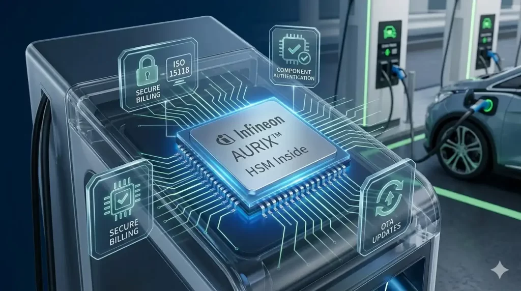
The Security Control Hub of Fast Charging Piles: Decoding AURIX™ MCU and Hardware Encryption