Wide Bandgap Revolution: Core Advantages and Design Challenges of GaN and SiC Power Semiconductors

The landscape of power electronics is undergoing a fundamental structural shift. For decades, Silicon (Si) has been the bedrock of power conversion, from the humble MOSFET in consumer adapters to the massive IGBT modules driving industrial traction. However, as global demands for power density and energy efficiency approach the theoretical limits of silicon physics, Wide Bandgap (WBG) materials—specifically Gallium Nitride (GaN) and Silicon Carbide (SiC)—have emerged not merely as alternatives, but as essential enablers for the next generation of power systems.
For the practicing design engineer, the migration to WBG is rarely a simple component swap. It requires a holistic rethinking of the power stage, encompassing gate drive topologies, PCB layout minimization, and thermal management. This article provides a rigorous technical examination of the trade-offs between Si, SiC, and GaN, and details the specific engineering challenges involved in implementing these high-speed devices.
I. The Triad of Power: Si, SiC, and GaN Positioning
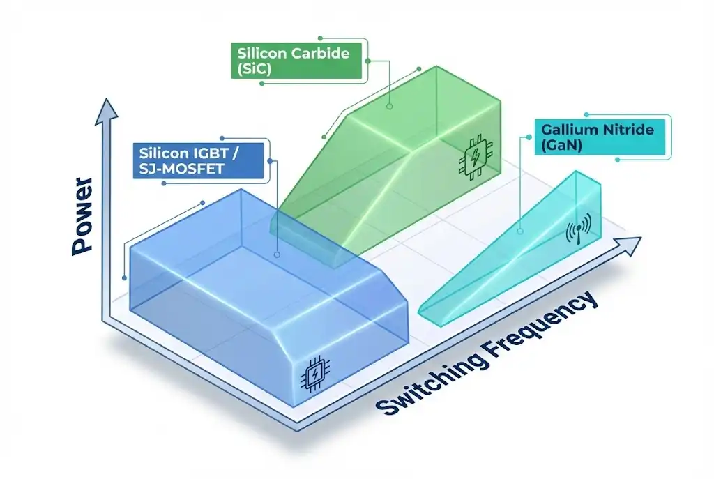
To select the correct semiconductor, engineers must first understand the “sweet spot” for each technology. The market has segmented based on voltage ratings, switching frequency capabilities, and thermal conductivity.
- Gallium Nitride (GaN): The Speed Demon. GaN offers the highest electron mobility, allowing for extremely fast switching speeds (often >100 V/ns). It is the technology of choice for applications requiring ultimate power density, such as server power supply units (PSUs) and compact DC-DC converters. Its lateral structure allows for chip-scale packaging, virtually eliminating package parasitics.
- Silicon Carbide (SiC): The High-Voltage Workhorse. SiC excels in high-voltage (>900V) and high-temperature environments. With a thermal conductivity roughly three times that of silicon, it is ideal for harsh environments like automotive traction inverters and grid-tied solar inverters.
- Silicon (Si): The Cost-Performance Baseline. Despite the rise of WBG, Silicon IGBTs and Superjunction MOSFETs remain dominant in cost-sensitive, lower-frequency applications (< 20 kHz), such as standard industrial motor drives and white goods.
For a detailed breakdown of the physical property differences between these materials, you can refer to our technical analysis: The Silicon Barrier: A Technical Showdown of Si MOSFET vs SiC and GaN.
II. Technical Performance Comparison: The Physics of Efficiency
The superiority of WBG materials stems from their bandgap energy, but the practical advantages are best understood through specific dynamic parameters: Reverse Recovery Charge (Qrr) and Breakdown Field Strength.
1. The Zero Qrr Advantage of GaN

In hard-switching topologies, such as the continuous conduction mode (CCM) totem-pole PFC, the reverse recovery of the body diode is a primary loss mechanism. When a switch turns on while the opposing body diode is conducting, the diode must flush out its stored minority carriers before it can block voltage. This creates a significant current surge, leading to high switching losses and electromagnetic interference (EMI).
GaN HEMTs (High Electron Mobility Transistors) are fundamentally different. They are majority carrier devices with no PN junction body diode. Consequently, they exhibit zero reverse recovery charge (Qrr = 0). This absence of Qrr allows GaN to operate in hard-switching topologies at frequencies that would destroy silicon devices due to thermal runaway.
2. SiC vs. Silicon Superjunction
While SiC MOSFETs do possess a body diode, their performance is vastly superior to Silicon. A typical 600V Silicon Superjunction MOSFET might have a Qrr of 860 nC or higher at 25°C. In contrast, a comparable SiC MOSFET often exhibits a Qrr of less than 40 nC. This reduction by a factor of 20 allows SiC to reduce switching losses (Eon) significantly, enabling higher switching frequencies and smaller passive components.
For further reading on material properties, the IEEE Xplore Digital Library offers extensive research papers detailing the characterization of WBG wide bandgap semiconductors.
3. Temperature Stability: RDS(on)
Engineers must carefully consider the temperature coefficient of the on-resistance (RDS(on)).
SiC: Exhibits excellent stability. The RDS(on) at 150°C is typically only 1.3 to 1.5 times the value at 25°C.
GaN: Has a steeper curve, with RDS(on) at 150°C potentially reaching 2.0 to 2.4 times the room temperature value. This necessitates a more conservative thermal design to ensure the device stays within its efficient operating window.
III. The Silicon Defender: When to Stick with IGBTs
It is crucial not to view WBG as a universal replacement. In the realm of high-power electric vehicle inverters and industrial motor drives, Silicon IGBTs often remain the engineering choice.
1. Short Circuit Robustness in Motor Drives
In traction inverters and industrial servo drives, the load (the motor) is remote and subject to insulation failure or cable damage. The power semiconductor must be able to withstand a direct short circuit across the DC bus for a specific duration—typically 10 microseconds (µs)—to allow the gate driver’s desaturation protection to detect the fault and safely shut down the system.
Modern IGBTs, such as the Infineon IGBT7 series, are specifically designed to balance VCE(sat) against this short-circuit capability. While SiC devices are improving in this regard, Silicon IGBTs generally offer a higher short-circuit withstand time (tSC) and a larger thermal mass, making them more forgiving in catastrophic fault scenarios.
To understand the specific trade-offs in EV powertrain applications, see our guide: SiC vs. IGBT: The Technology Showdown Powering the Future of EVs.
2. The Frequency Factor
If the application switches below 20 kHz (common for large motors to protect bearings and insulation), the dynamic switching losses reduced by SiC or GaN are negligible compared to the static conduction losses. In these cases, the low VCE(sat) of an IGBT provides the best efficiency per dollar. Selecting the right device requires analyzing the crossover point where switching losses overtake conduction losses.
For high-frequency designs where IGBTs might struggle, consult: IGBT Selection: Beyond Vcesat for High-Frequency Designs.
IV. GaN Design Mastery: Addressing Layout and Drive Challenges
Designing with GaN is often described as “Formula 1 engineering.” The performance is incredible, but the margin for error is razor-thin. The primary challenges revolve around the sensitivity of the gate and the parasitic inductance of the layout.
1. Gate Injection Transistors (GIT) vs. MOSFETs
Many GaN devices, particularly those from manufacturers like Infineon (CoolGaN), utilize a p-GaN gate structure known as a Gate Injection Transistor (GIT). Unlike a standard voltage-driven MOSFET, a GIT is technically a current-driven device.
The gate behaves like a diode with a forward voltage drop of approximately 3.0V to 3.5V. To keep the device on, a continuous “holding current” (typically a few milliamps) is required. To switch it on quickly, a high transient current is needed to charge the gate capacitance. This is achieved using a specialized RC network in the gate drive path. The capacitor allows the transient current spike for fast dV/dt, while the resistor limits the steady-state current. Engineers cannot simply connect a standard 15V MOSFET driver to a GaN HEMT; doing so would destroy the gate immediately.
Reference technical data from EPC (Efficient Power Conversion) provides excellent depth on the physics of GaN gate structures.
2. The Law of Inductance: V = L × di/dt
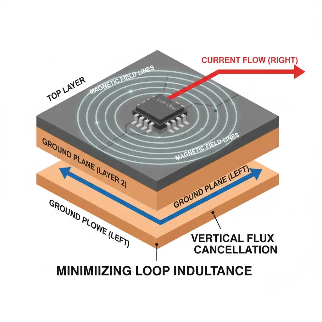
The most critical equation in GaN design is the inductive voltage spike equation. With GaN devices capable of switching current at rates (di/dt) exceeding 3000 A/µs, even 1 nH of parasitic inductance becomes problematic.
Example Calculation:
If Lloop = 5 nH and di/dt = 2000 A/µs (or 2 A/ns):
Vspike = 5 nH × 2 A/ns = 10 V.
A 10V spike on the gate can exceed the breakdown voltage, and on the drain, it adds to the blocking voltage stress. To mitigate this, the “Power Loop” (the path from the DC bus capacitor, through the high-side switch, low-side switch, and back) must be minimized.
Layout Best Practice: The most effective method to reduce loop inductance is vertical cancellation. By placing the DC bus capacitors on the bottom layer of the PCB directly underneath the GaN switches on the top layer, the magnetic fields generated by the outgoing and returning currents cancel each other out. This can reduce loop inductance to as low as 0.4 nH.
3. Thermal Management and Top-Side Cooling
Standard bottom-side cooled packages (like TO-247) rely on the PCB for heat spreading or through-hole mounting. This conflicts with the need for tight electrical layout. Modern GaN devices often employ top-side cooling. The heat is extracted from the top of the package directly to a heatsink, leaving the bottom side of the package strictly for electrical connections. This decouples the thermal and electrical design, allowing for the tightest possible component placement.
V. Measurement Challenges: The “Ghost” Signals

Validating a GaN design is notoriously difficult because standard lab equipment often lies to you. The speeds involved expose the limitations of traditional voltage probes.
1. Bandwidth Requirements
Engineers often assume that if their switching frequency is 500 kHz, a 100 MHz oscilloscope is sufficient. This is incorrect. The required bandwidth is determined by the rise time (tr), not the switching frequency.
The approximate relationship is: Bandwidth = 0.35 / tr.
For a GaN device with a 2 ns rise time, the required system bandwidth is approximately 175 MHz just to see the fundamental edge. However, to accurately capture the overshoot and ringing (which are critical for reliability), a bandwidth of 500 MHz to 1 GHz is recommended.
2. Common Mode Transient Immunity (CMTI)
The most challenging measurement is the high-side Gate-Source voltage (VGS). The source of the high-side switch is the switching node, which might be jumping from 0V to 400V in 5 nanoseconds. This represents a dv/dt of 80 V/ns.
Traditional differential probes have parasitic capacitance between the inputs and ground. This high dv/dt drives current through that parasitic capacitance, generating a voltage error that appears as noise on the oscilloscope. This is often misinterpreted as gate ringing.
To see the true signal, engineers must use optically isolated probes (such as the Tektronix IsoVu system). These probes use fiber optics to transmit the signal, providing virtually infinite isolation and eliminating the common-mode error.
For more on high-performance measurement techniques, reliable information can be found via Tektronix Isolated Probes.
Conclusion
The transition to Wide Bandgap semiconductors is a transformative step for the power electronics industry. GaN and SiC are not just “better silicon”; they are distinct technologies that solve different problems. SiC dominates the high-voltage, high-temperature domain of electric mobility, while GaN rules the high-density, high-frequency landscape of data centers and consumer electronics.
However, extracting the performance promised by data sheets requires a rigorous engineering approach. It demands a deep understanding of device physics, a mastery of low-inductance PCB layout, and the use of advanced measurement instrumentation. For the power engineer, the learning curve is steep, but the reward—systems that are smaller, lighter, and more efficient than ever before—is well worth the climb.
Explore more technical resources on power semiconductor applications at the SLW Electronics Engineering Hub.
Further Reading & Industry References
- Wolfspeed. (n.d.). Silicon Carbide Power MOSFETs and Diodes. https://www.wolfspeed.com
- Infineon Technologies. (n.d.). CoolGaN™ Gallium Nitride HEMT Technology. https://www.infineon.com
Content in This Series

Si vs. SiC vs. GaN: A Technical Deep Dive into Switching Speed and Power Losses

Designing High-Performance GaN Circuits: Mastering Gate Drive, Layout, and Signal Integrity