Debunking the Myth: In Solar Inverter IGBT Selection, Focusing Only on VCE(sat) is a Losing Strategy
In my 15 years as an application engineer, I’ve seen countless engineers, especially early in their careers, fall into a common trap when selecting IGBTs. They open a few datasheets, scroll directly to the VCE(sat) specification, and assume, “the lower the saturation voltage, the lower the module’s power loss, and thus the higher the efficiency.” This logic might barely hold up if your project is a 50Hz industrial motor drive. But if you’re designing a modern solar inverter, where efficiency and power density are paramount, I have to tell you: this mindset will not only put you behind from the start, but it could also drag your entire project into a thermal design nightmare, completely undermining your goals of high efficiency and high power density.
Let’s make this challenge tangible. Picture an engineer named Li, who is working on a new 100kW three-phase string solar inverter. His core KPIs are to increase the peak efficiency from the previous generation’s 98.2% to over 98.6%, while also reducing the overall cost and size to stay competitive. To shrink the expensive and bulky DC and AC inductors, he plans to increase the switching frequency (f_sw) from a conservative 12kHz to a more aggressive 16-20kHz. However, his initial simulations deliver a harsh reality check: the heatsink temperature soars, and system efficiency drops instead of rising. This is the classic “Frequency-Efficiency-Cost” trilemma, and the key to solving it lies in a deep understanding of IGBT loss components.
The Core Principle: Conduction Loss vs. Switching Loss – The Main Battlefield in High-Frequency Applications
The total losses in any power electronic converter are primarily composed of two parts: Conduction Loss and Switching Loss. Their characteristics are fundamentally different:
- Conduction Loss: Primarily determined by the IGBT’s saturation voltage (VCE(sat)) and the diode’s forward voltage (Vf). It occurs when the IGBT is fully on, and its power is approximately VCE(sat) × I_c × DutyCycle. For a given current, it’s almost a constant and is independent of the switching frequency.
- Switching Loss: Comprised of the energy lost during the IGBT turn-on (Eon) and turn-off (Eoff) events. It only occurs during the nanosecond-scale switching transitions, but its total power is P_sw ≈ (Eon + Eoff) × f_sw. This means switching loss is strictly proportional to the switching frequency.
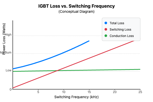
In low-frequency applications (e.g., <5kHz), switching events are infrequent, and conduction loss dominates. Therefore, focusing on VCE(sat) is reasonable. But in applications like solar inverters, with frequencies often at 16kHz, 20kHz, or even higher, the device switches tens of thousands of times per second. Switching losses accumulate rapidly and often surpass conduction losses, becoming the main contributor to total loss and system temperature rise. As the chart below illustrates, the steep rise in switching loss is the fundamental bottleneck limiting high-frequency design.
Therefore, our selection logic must be completely re-framed: For a high-frequency solar inverter, an ideal IGBT should have the “lowest possible” switching loss (Eon and Eoff) built upon a foundation of a “good enough” VCE(sat).
Deep Dive: How the FF450R12KE4 Solves the “Frequency-Efficiency-Cost” Trilemma
Now, let’s focus on a star module from Infineon: the FF450R12KE4. This 1200V/450A module, housed in the industry-acclaimed EconoDUAL™ 3 package, is built on Infineon’s IGBT4 Trench-Field-Stop chip technology. Setting aside the marketing terms, the core advantage of this technology is its near-perfect balance between VCE(sat) and switching loss, making it tailor-made for high-frequency hard-switching applications like solar inverters and UPS systems.

Let’s use data to see how it helps our engineer, Li. Assuming a simplified 100kW inverter operating condition:
| Key Parameter | FF450R12KE4 Typical Value (Tj=125°C) | Practical Implication for a 100kW/16kHz Inverter (So What?) |
|---|---|---|
| VCE(sat) @ 450A | 1.85V | Provides a sufficiently low conduction loss to ensure baseline efficiency at full load. It’s not the industry’s lowest, but it’s a carefully engineered trade-off to allow for superior switching performance. |
| Eon (Turn-on Energy) | 52 mJ | This is the core of the solution! Lower Eon means less thermal stress during each turn-on event. At 16kHz, this directly translates to lower heat generation. |
| Eoff (Turn-off Energy) | 60 mJ | Equally critical for high-frequency performance. The IGBT4 technology optimizes the turn-off tail current, significantly reducing Eoff and thus saving substantial losses at high frequencies. |
| Rth(j-c) (Junction-to-Case Thermal Resistance) | 0.040 K/W per switch | This is the unsung hero. An extremely low thermal resistance ensures that heat generated at the chip junction is efficiently transferred to the heatsink. This means a lower chip temperature for the same power dissipation, leading to higher reliability and a longer lifetime. |
For Li’s design, choosing the FF450R12KE4 means that when he increases f_sw from 12kHz to 16kHz, the corresponding increase in switching loss, dictated by (Eon + Eoff) × f_sw, will be kept within a manageable range. This gives him enough thermal design margin to successfully achieve system miniaturization without sacrificing precious efficiency points.
Beyond the Module: The Importance of Gate Drive and Layout
A seasoned engineer knows that a component’s maximum performance is defined by the device itself, but whether that potential is reached depends on the external circuit. Choosing the FF450R12KE4 is only half the battle; the other half is:
- Gate Drive: The excellent switching characteristics of the FF450R12KE4 require a “fast, precise, and stable” gate drive circuit to match. The right gate resistor (Rg)—not too large, not too small—and sufficient drive current capability are crucial for unlocking its full low-Eon/Eoff potential.
- Power Loop Layout: At 16kHz or higher, stray inductance (Lσ) in the power loop can cause significant voltage overshoot (V = Lσ × di/dt). Low-inductance packages like the EconoDUAL™ 3 help, but engineers must still minimize its impact through optimized PCB layout (e.g., using laminated bus bars). Otherwise, voltage spikes could damage the module.
Frequently Asked Questions (FAQ)
Q: What is Trench-Field-Stop technology?
A: It’s a key technology in modern IGBT chip design, best understood as a combination of two techniques:
- Trench Gate: Compared to a traditional planar gate structure, a trench structure allows for a much higher density of cells arranged vertically on the chip surface. The direct benefit is a lower on-state resistance for the same chip area, which reduces VCE(sat).
- Field-Stop Layer: An additional “N” buffer layer is added to the back of the chip. Its function is to abruptly “stop” the electric field from extending through the device during turn-off, allowing the chip to be made much thinner. A thinner chip means less stored charge, which significantly reduces the “tail current” during turn-off, directly lowering the turn-off loss (Eoff).
In short, Trench technology primarily optimizes conduction loss, while Field-Stop technology primarily optimizes switching loss. The combination of the two is the secret behind how modules like the FF450R12KE4 achieve their excellent balance between VCE(sat) and E_sw.
Q: Besides solar inverters, where else can the FF450R12KE4 be used?
A: Any hard-switching topology that demands high efficiency, high power density, and high switching frequency is an ideal application for the FF450R12KE4. Typical applications include:
- Uninterruptible Power Supplies (UPS): Especially high-power online UPS systems for data centers.
- Industrial Drives: High-performance servo drives and general-purpose inverters.
- High-Frequency Induction Heating and Welding: These applications require extremely fast switching for precise control.
- Commercial and Construction Vehicle Drives: Electric drivetrains for electric buses, forklifts, etc.
Conclusion and Final Call to Action
IGBT selection is both an art and a science, requiring engineers to have a holistic view and a deep understanding of their application. For modern solar inverter design, the “VCE(sat)-only” approach is obsolete. Embracing the philosophy of “total loss optimization” is the correct path to success.
The value of a module like the FF450R12KE4 lies not in the extremity of any single parameter, but in the masterful balance between all key parameters (VCEsat, Eon, Eoff, Rth). It provides system engineers with a powerful weapon to solve the “Frequency-Efficiency-Cost” trilemma.
Stop letting outdated selection logic slow down your project. Download the official datasheet for the FF450R12KE4 now and run a targeted calculation using the manufacturer’s online simulation tools. Arm your design decisions with real numbers and loss simulations. If you encounter any challenges during selection or simulation, our team is ready to provide application support to help you choose the best power semiconductor solution for your project.