DIY a High-Power SMPS: IGBT Selection and Circuit Construction Guide (2025 Q3)
The Allure and Pitfalls of Building Your Own High-Power SMPS
Embarking on a project to build a high-power Switched-Mode Power Supply (SMPS) is a rite of passage for many electronics engineers and serious hobbyists. Whether for a custom lab bench supply, a high-frequency induction heater, or an experimental EV charging station, the appeal of crafting a power source tailored to your exact needs is undeniable. However, the path from concept to a stable, efficient, and safe power supply is fraught with challenges. The heart of any high-power SMPS is the switching element, and for applications pushing kilowatts, the Insulated Gate Bipolar Transistor (IGBT) is often the component of choice.
The primary pitfall isn’t just in the complexity of the control logic, but in the nuanced and critical process of selecting the right IGBT and building the support circuitry around it. A poor choice can lead to immediate, catastrophic failure—a puff of smoke and a dead transistor. A suboptimal design might result in excessive heat, poor efficiency, and unacceptable electromagnetic interference (EMI). This guide provides a practical, engineering-focused walkthrough of the key decisions you’ll face, from topology selection to the nitty-gritty details of IGBT selection and circuit construction.
Foundational Choice: Selecting the Right SMPS Topology
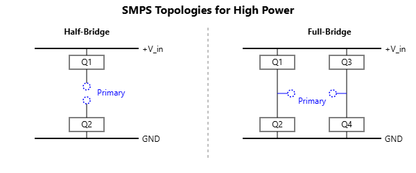
Before you can even think about which IGBT to use, you must decide on the power stage topology. For high-power applications (typically >1kW), the choice often boils down to two primary contenders: the Half-Bridge and the Full-Bridge converter. While other topologies exist, these two provide an excellent balance of performance and manageable complexity.
[SVG_SMPS_Topologies_Diagram]
The choice between them depends heavily on your specific power requirements and input voltage source.
| Topology | Pros | Cons | Best For |
|---|---|---|---|
| Half-Bridge |
|
|
Cost-sensitive applications, moderate power levels (e.g., 500W to 2kW). |
| Full-Bridge |
|
|
High-power applications (>2kW), such as welding supplies, high-power motor drives, and large inverters. |
For a truly “high-power” DIY project, the Full-Bridge topology is generally the superior choice. It allows you to extract more power from your transformer and places less current stress on the IGBTs compared to a Half-Bridge at the same power level. The rest of this guide will assume a Full-Bridge design.
A Practical Guide to Selecting the Perfect IGBT
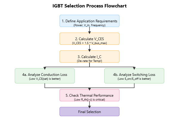
Choosing the right IGBT is not about finding the one with the highest ratings. It’s a balancing act of several key parameters to match your specific application’s needs. A systematic approach is crucial to avoid costly mistakes.
1. Collector-Emitter Voltage (V_CES)
This is your first filter. The V_CES rating must be able to withstand the maximum DC bus voltage plus any voltage overshoots caused by switching. A common rule of thumb is to select an IGBT with a V_CES rating of at least 1.5 to 2 times your maximum DC bus voltage. For a 400V DC bus, a 600V IGBT might be marginal, making a 1200V IGBT a much safer and more robust choice. Don’t skimp on this safety margin; transient voltage spikes are a primary cause of IGBT failure.
2. Continuous Collector Current (I_C)
The I_C rating must exceed the maximum RMS current your IGBT will see in operation. This requires calculating the primary current based on your output power, efficiency, and input voltage. Remember that the I_C rating in datasheets is often specified at a case temperature of 25°C, which is unrealistic. You must de-rate the current capability based on your expected operating case temperature (e.g., 100°C). Always look for the I_C rating at this higher temperature in the datasheet graphs.
3. Saturation Voltage (V_CE(sat))
This parameter is directly tied to conduction losses (P_cond = V_CE(sat) * I_C * Duty Cycle). A lower V_CE(sat) means less power dissipated as heat during the on-state, leading to higher efficiency and easier thermal management. However, there is often a trade-off: IGBTs with very low V_CE(sat) might have slower switching speeds, leading to higher switching losses. For SMPS designs operating at tens of kilohertz, you must balance these two factors.
4. Switching Speed (E_on, E_off, t_r, t_f)
Switching losses are a function of switching frequency and the energy lost during turn-on (E_on) and turn-off (E_off). Faster rise (t_r) and fall (t_f) times reduce these losses. However, extremely fast switching can exacerbate EMI and cause more severe voltage overshoots due to stray inductance in your layout. For a hard-switched full-bridge operating between 20-50 kHz, you don’t need the absolute fastest IGBT on the market. A well-balanced device is better than an ultra-fast one that is difficult to control.
5. Thermal Resistance (R_th(j-c))
This specification dictates how efficiently heat can be transferred from the semiconductor junction to the device case. A lower Thermal Resistance is always better. It means for a given power dissipation, the junction temperature will be lower, increasing reliability and lifetime. This parameter is critical for calculating your heatsink requirements.
6. Package Type
For lower-power builds, discrete packages like TO-247 are common. However, as power levels climb into the multi-kilowatt range, building a full bridge with four discrete devices becomes a thermal and layout nightmare. This is where IGBT modules, such as the FF450R12KE4, shine. They integrate a half-bridge or full-bridge configuration into a single, thermally efficient package. This simplifies mounting to a heatsink, minimizes stray inductance between switches, and ensures the devices are closely matched.
Essential Circuits: Mastering the Gate Drive, Snubber, and Thermal Design
Selecting the right IGBT is only half the battle. The surrounding circuitry is what enables it to perform reliably.
The Gate Driver: The Brains Behind the Brawn
You cannot drive a high-power IGBT directly from a microcontroller. A dedicated Gate Drive circuit is mandatory. Its key functions are:
- High Peak Current: To charge and discharge the IGBT’s gate capacitance quickly for efficient switching.
- Isolation: To separate the low-voltage control side from the high-voltage power stage.
- UVLO (Under-Voltage Lockout): To prevent the IGBT from operating with insufficient gate voltage, which can cause it to enter the linear region and rapidly overheat.
- Negative Gate Voltage: Providing a negative voltage (e.g., -5V to -15V) during the off-state provides a strong defense against parasitic turn-on caused by the Miller effect, especially during the fast turn-on of the opposing switch in a bridge leg.
For more insights on this critical component, consider these 5 practical tips for robust IGBT gate drive design.
Snubber Circuits: Taming Destructive Voltage Spikes
Every wire, trace, and component lead has stray inductance. When you abruptly turn off the current flowing through an IGBT, this inductance generates a large voltage spike (V = L * di/dt). This spike can easily exceed the IGBT’s V_CES rating and destroy it. A Snubber Circuit, typically an RCD (Resistor-Capacitor-Diode) network placed across each IGBT, absorbs the energy from this spike, clamping the voltage to a safe level.
Thermal Management: The Unsung Hero
Heat is the enemy of all power electronics. Your thermal design is just as important as your electrical design.
- Calculate Total Losses: Sum the conduction losses and switching losses to find the total power dissipated by each IGBT.
- Select a Heatsink: Use the IGBT’s R_th(j-c), the thermal resistance of your thermal interface material (TIM), and your calculated power loss to determine the required thermal resistance of the heatsink (R_th(s-a)).
- Consider Airflow: Don’t forget that heatsink ratings are often specified with forced airflow. A fan can dramatically improve thermal performance and allow for a smaller, more compact design.
Troubleshooting Common Failures in Your DIY SMPS Build
Even with careful design, things can go wrong. Here are some common failure modes and their likely causes.
| Problem | Likely Causes | Solutions |
|---|---|---|
| Instant IGBT Failure on Power-Up | Shoot-through (both IGBTs in a leg on simultaneously), gate oscillation, exceeding the SOA (Safe Operating Area). | Implement robust dead-time in your PWM controller. Optimize gate resistor value. Check for and eliminate layout issues like long gate drive traces. |
| Rapid Overheating | Inadequate heatsinking, insufficient gate drive voltage (leading to high V_CE(sat)), excessive switching frequency for the chosen IGBT. | Re-evaluate thermal calculations. Ensure your gate driver provides the recommended voltage (e.g., +15V). Consider an IGBT with lower V_CE(sat) or lower switching losses, like a module from the BSM series. Reduce operating frequency. |
| Audible Whining or Instability | Control loop instability, flux saturation in the transformer, sub-harmonic oscillation. | Check your feedback compensation network. Verify your transformer design has sufficient headroom. Ensure your PWM duty cycle is properly limited. |
| High EMI/Noise | Poor PCB layout with large current loops, overly fast switching, inadequate snubbing. | Minimize the area of high-frequency current loops. Add or tune snubber circuits. Use appropriate gate resistors to slightly slow down switching edges. Add input and output filtering. |
Final Checklist for a Successful High-Power SMPS Project
Building a high-power SMPS is a rewarding challenge that pushes your engineering skills. By following a systematic and cautious approach, you can dramatically increase your chances of success. Before you power on your creation, run through this final checklist:
- ✅ Topology Confirmed: Full-Bridge chosen for high-power capability.
- ✅ IGBTs Correctly Sized: V_CES, I_C, and thermal ratings verified with safety margins.
- ✅ Gate Drive is Robust: Isolated, provides sufficient current, and uses a negative turn-off voltage.
- ✅ Protection is in Place: Snubber circuits are installed, and dead-time is correctly implemented.
- ✅ Thermal Management is Adequate: Heatsink is properly sized and mounted with quality thermal paste.
- ✅ Layout is Optimized: Power loops are tight, and gate drive traces are short and clean.
A successful DIY power supply project hinges on understanding the critical role of the IGBT and designing the entire system to support it. For sourcing high-quality, reliable IGBT modules for your most demanding projects, from brands like Infineon, Mitsubishi, and Fuji, browse the extensive selection available at SLW-ELE.COM.