In the rapidly evolving landscape of electrified transportation—spanning high-speed rail networks, urban light transit, heavy-duty commercial electric vehicles, and modern automotive traction systems—engineers are continuously fighting a battle for higher power density and greater system efficiency. The heart of these vehicular drive systems is the traction converter, a critical power electronics unit responsible for transforming direct current (DC) from a battery or overhead line into variable-frequency alternating current (AC) to drive the traction motors.
As the industry transitions toward high-speed silicon insulated-gate bipolar transistors (IGBTs)—which engineers can explore further in this in-depth analysis of IGBT modules—and next-generation silicon carbide (SiC) metal-oxide-semiconductor field-effect transistors (MOSFETs), a hidden physical barrier has become the primary limiting factor in converter design: stray inductance.
Stray inductance, often referred to as parasitic inductance, is the unavoidable inductance that exists in the conductive tracks, wires, and component terminals of any electrical circuit. In low-power electronics, it is often negligible. However, in megawatt-scale traction converters switching thousands of amperes in a matter of nanoseconds, stray inductance becomes a destructive force. This article provides a deep, objective engineering analysis of the physical paths to minimize stray inductance, exploring advanced structural concepts such as laminated busbar magnetic cancellation and topological optimizations like the XHP™ terminal arrangement.
The Physics of the Problem: Why Stray Inductance Matters in Power Commutation
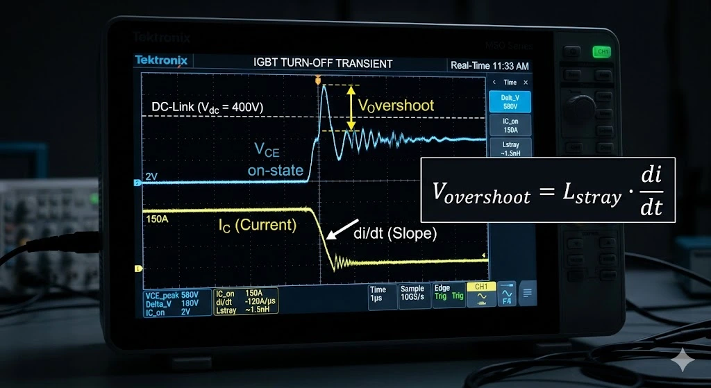
To understand the profound urgency of minimizing stray inductance, one must look at the fundamental electrical behavior of switching power semiconductors. When a power module turns off, the massive current flowing through the device drops from its nominal operating value to essentially zero in an incredibly short timeframe. This rate of change of current over time is denoted in engineering as di/dt.
According to Faraday’s law of induction, any change in current through an inductive loop generates an electromotive force (EMF) that opposes the change. In the context of a traction converter’s DC-link circuit, this is mathematically expressed by the fundamental equation:
Vovershoot = Lstray · (di / dt)
Where:
- Vovershoot is the induced transient voltage spike across the semiconductor device during turn-off.
- Lstray is the total parasitic inductance of the commutation loop. This includes the internal equivalent series inductance (ESL) of the DC-link capacitors, the inductance of the busbar connecting the capacitors to the modules, and the internal packaging inductance of the power module itself.
- di / dt is the rate of current decrease during the switching event.
The peak voltage experienced by the semiconductor (VCE(peak) for an IGBT, or VDS(peak) for a MOSFET) is the sum of the steady-state DC bus voltage (VDC) and this induced transient overshoot:
VCE(peak) = VDC + Vovershoot
If VCE(peak) exceeds the physical breakdown voltage rating of the semiconductor chip—for instance, when designing high-voltage systems using industry-standard modules like the Infineon FS450R17KE3—the device will suffer avalanche breakdown and catastrophic failure. Modern wide-bandgap devices like SiC MOSFETs are highly prized for their ability to switch incredibly fast, yielding a very high di/dt.
While this fast switching drastically reduces dynamic energy losses, it proportionately inflates the voltage overshoot unless the physical Lstray of the system is aggressively minimized.
Therefore, eliminating stray inductance is not merely a marginal optimization; it is a fundamental prerequisite for utilizing modern, high-speed power semiconductor devices safely and effectively. Designers cannot fully leverage the benefits of advanced silicon or silicon carbide without first solving the physical geometry of the commutation loop.
Harnessing Magnetic Cancellation: The Engineering of the Laminated Busbar
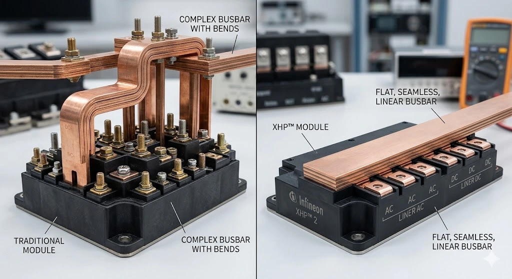
The traditional method of connecting the DC-link capacitor bank to the power semiconductor modules in legacy converters involved using thick, round copper cables or standalone, separated copper bars. These discrete conductors form a large spatial loop area. Because inductance is geometrically tied to the area enclosed by a current loop, these legacy designs inherently possess unacceptably high stray inductance—often in the range of hundreds of nanohenries (nH).
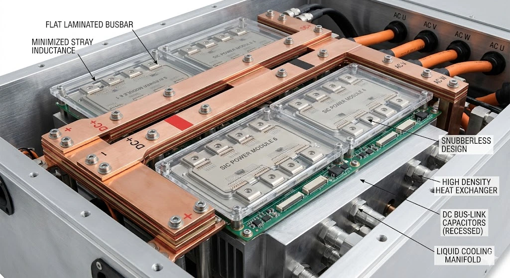
The modern engineering solution to this physical problem is the laminated busbar. A laminated busbar replaces discrete, separated wires with wide, flat conductive plates (usually highly conductive copper or lightweight aluminum) that are stacked tightly on top of one another. These conductive layers are separated by ultra-thin, high-dielectric-strength insulating materials such as PET (Polyethylene terephthalate), PEN (Polyethylene naphthalate), or Polyimide (Kapton). This tight, sandwich-like construction relies on a profound electromagnetic phenomenon: magnetic cancellation.
The Mechanism of Destructive Interference
When the traction inverter is operating, the positive plate of the busbar carries current from the DC-link capacitor to the power module, while the negative plate carries the exact same magnitude of current back from the module to the capacitor. According to Ampere’s Law and the right-hand grip rule, a current-carrying conductor generates a magnetic field circulating around it.
Because the currents in the closely spaced positive and negative plates flow in perfectly opposite directions, the magnetic flux vectors generated by these two plates are oriented in opposite directions. Since the physical separation between the plates is extremely small (often less than 1 millimeter of dielectric material, depending on the isolation voltage requirement), the two opposing magnetic fields occupy virtually the same spatial volume. Consequently, they undergo destructive interference—they cancel each other out.
The equivalent inductance of a parallel plate transmission line can be approximated by its physical dimensions:
L ≈ (μ0 · d · l) / w
Where:
- μ0 is the magnetic permeability of the insulating medium.
- d is the thickness of the dielectric insulation (the physical distance between the conductive plates).
- l is the length of the busbar path.
- w is the width of the conductive plates.
This mathematical relationship reveals the definitive path to physical minimization: to achieve the lowest possible inductance, mechanical engineers must maximize the width of the plates (w) and their overlapping area, while radically minimizing the insulation thickness (d) without compromising the high-voltage isolation and partial discharge requirements of the traction system.
High-quality laminated busbars can reduce the commutation loop inductance to the exceptionally low range of 10 to 30 nH, representing a reduction of nearly 90% compared to traditional cabling. Furthermore, this tight parallel-plate geometry naturally forms a distributed capacitor. This intrinsic, albeit small, capacitance acts as an integrated high-frequency bypass filter, absorbing localized high-frequency voltage ripples right at the source and further stabilizing the DC link.
Topological Evolution: The XHP™ Terminal Advantage
While optimizing the external laminated busbar is a critical step, the engineering effort is severely compromised if the power semiconductor module itself forces the current to travel through inefficient, high-inductance internal geometries. Legacy or standard high-power module packaging—even highly reliable workhorses like the Infineon FF600R12IP4 often utilized in wind turbines—historically featured offset, asymmetric terminal layouts. Connecting a perfectly flat, low-inductance laminated busbar to these awkward screw terminals required the busbar to twist or bend.These mechanical adaptations inadvertently reintroduced “open air” inductive loops right at the critical point of connection.
To overcome this packaging limitation, the industry—initially spearheaded by major semiconductor manufacturers and subsequently adopted as an open, standardized footprint—developed the High Power Next Generation (XHP™) packaging topology. XHP packaging represents a fundamental shift in the electromechanical design of high-power traction modules, specifically engineered for demanding voltage classes from 1.7kV up to 6.5kV. For a comprehensive look at how this impacts system architecture, engineers can explore the peak performance of traction converters by decoding the XHP platform.
The Symmetrical Strip-Line Concept
The topological brilliance of the XHP module lies in its strict terminal symmetry and logical phase segregation. In an XHP package, the DC+ and DC- terminals are placed directly adjacent to one another in a straight line on one specific side of the module, while the AC output terminals are located entirely on the opposite side. This layout provides two massive advantages for stray inductance minimization:
- Direct Planar Connection: Because the DC terminals are linearly aligned and closely paired, the laminated busbar can connect to the module without any spatial distortion, twisting, or bending. The positive and negative plates of the busbar remain perfectly parallel all the way to the mounting screws, ensuring that the magnetic cancellation effect is maintained continuously from the capacitor bank right up to the module housing.
- Internal Strip-Line Design: The physical layout benefits do not stop at the external plastic casing. Inside the XHP module, the conductive routing from the external terminals down to the Direct Copper Bonded (DCB) ceramic substrates mirrors the external busbar. It utilizes an internal “strip-line” architecture—essentially a miniaturized laminated busbar built directly into the module’s framework—which prevents the positive and negative current pathways from separating until the very last moment before reaching the semiconductor dies.
This holistic, end-to-end approach effectively eliminates the stray inductance historically caused by complex internal wiring crossovers and asymmetric terminal placements. When designing a megawatt-scale traction converter, specifying topologically symmetrical packages like the XHP is just as vital as the meticulous design of the external busbar itself.
Decoupling Voltage Overshoot and Switching Speed
The physical minimization of stray inductance through precise laminated busbars and XHP packaging yields its most profound reward in the dynamic electrical behavior of the converter. It fundamentally alters the traditionally restrictive relationship between voltage overshoot and switching speed.
In power electronics gate drive design, controlling the turn-off behavior is primarily managed by adjusting the gate resistor (Rg). The gate resistor limits the current that charges and discharges the semiconductor’s internal gate capacitance (including the critical Miller capacitance). If a system suffers from high physical stray inductance, the designer is forced into a corner: they must increase the value of Rg(off). A higher gate resistance slows down the extraction of gate charge, which subsequently slows down the transition of the collector or drain current (effectively reducing the di/dt). By deliberately slowing down the switching speed, the V = L · (di/dt) equation is kept artificially in check, ensuring the voltage overshoot remains safely within the device’s Safe Operating Area (SOA).
However, this forced safety margin comes at a severe operational cost: immense thermal generation. Slower switching transitions mean the semiconductor spends a longer duration in the active (linear) region during every single switching cycle, where both voltage and current are simultaneously high. This drastically increases the switching energy loss during turn-off (Eoff). In a high-power traction inverter switching at several kilohertz, these amplified dynamic losses generate massive amounts of heat, necessitating larger liquid-cooling plates, heavier heat sinks, more powerful coolant pumps, and a generally bulkier thermal management system.
By drastically reducing Lstray at the structural level, this restrictive engineering compromise is broken. With a highly optimized, ultra-low-inductance commutation path, the voltage spike is intrinsically suppressed by the physics of the circuit rather than the artificial slowing of the gate drive. Consequently, the design engineer is granted the freedom to significantly decrease the gate resistance (Rg(off)). The semiconductor can be driven to switch at its maximum physical capability, experiencing extremely high di/dt, without the threat of a dangerous voltage overshoot. Understanding this dynamic is crucial when evaluating switching speed and power losses across Si, SiC, and GaN technologies.
The tangible result is a precipitous drop in dynamic switching losses. The semiconductor runs much cooler under identical load conditions, which extends its lifecycle, reduces thermal cycling stress on the solder joints and wire bonds, and significantly improves the overall reliability of the traction drive system under demanding acceleration and regenerative braking profiles.
System-Level Triumphs: Snubberless Design and Increased Power Density
The rigorous benefits of advanced physical structures cascade directly from the microsecond switching behaviors to the macroscopic system level, fundamentally altering the Bill of Materials (BOM), the cost structure, and the volumetric footprint of the entire traction converter.
Historically, to protect sensitive semiconductor devices from inductive voltage spikes in less-optimized layout geometries, power engineers were forced to implement “snubber” circuits. A snubber is an auxiliary passive circuit—typically a high-voltage, low-inductance film capacitor, often paired with high-wattage resistors and fast-recovery diodes to form an RCD network—placed directly across the DC terminals of the power module. The snubber acts as a localized energy absorber; when the semiconductor turns off abruptly, the inductive kickback current is briefly shunted into the snubber capacitor, physically clamping the voltage spike to a safe level.
While effective from an electrical protection standpoint, snubbers are highly undesirable mechanically, thermally, and economically. High-current, high-voltage snubber capacitors are physically bulky, heavy, and expensive. Furthermore, they are continuously subjected to intense high-frequency ripple currents. This leads to internal I2R heating due to the capacitor’s Equivalent Series Resistance (ESR), making them one of the most common thermal bottlenecks and points of failure in an inverter. The degradation of snubber capacitors directly reduces the Mean Time Between Failures (MTBF) of the entire rail or automotive vehicle.
Through the rigorous application of laminated busbar technology and low-inductance packaging like the XHP, the inherent stray inductance is driven so exceptionally low that the native voltage overshoot remains safely within the safety margin of the semiconductor’s blocking voltage, even at maximum switching speeds. This architectural perfection achieves what is often considered the “Holy Grail” of high-power converter design: a completely snubberless system.
Eliminating the snubber circuits frees up critical spatial volume inside the inverter housing. It dramatically reduces the overall weight of the traction unit—a crucial performance metric for electric multiple units (EMUs), high-speed rail, and battery electric vehicles (BEVs) where every kilogram saved translates directly to improved range and operational efficiency. Ultimately, the physical mitigation of stray inductance facilitates a massive leap in the volumetric (kW/liter) and gravimetric (kW/kg) power density of the converter.
Conclusion: The Physical Foundation of Electrical Efficiency
The relentless pursuit of efficiency, reliability, and miniaturization in modern electrified transportation systems cannot be solved by advancements in semiconductor physics alone. While the silicon or silicon carbide die acts as the active engine of the traction converter, its true operational performance is entirely constrained by the physical geometry of its surrounding environment. Stray inductance remains the primary bottleneck restricting the switching speeds and efficiency gains promised by next-generation power electronics.
As explored comprehensively in this engineering analysis, mitigating this bottleneck requires a multi-disciplinary approach rooted in rigorous mechanical and physical design. By deeply leveraging the electromagnetic principle of magnetic cancellation through tightly coupled, precision-engineered laminated busbars, and by adopting advanced, symmetrical packaging topologies like the XHP™ standard, engineers can successfully suppress commutation loop stray inductance to single-digit nanohenry levels.
This physical mastery completely decouples the traditional, limiting trade-off between switching speed and destructive voltage overshoot. It permits the use of lower gate resistance, enables much faster switching transitions, and drastically reduces dynamic thermal losses.
Ultimately, these optimized physical paths lead directly to the elimination of heavy, failure-prone snubber circuits. For design engineers and system architects navigating this complex ecosystem, prioritizing these structural layout principles is the absolute first step toward achieving a truly optimized power architecture. To further refine your component selection strategy, explore our head-to-head comparison of the Mitsubishi CM600DX-24T vs. Infineon FF600R12IP4 to understand how different manufacturer designs impact overall system efficiency.