The Advanced Thermal Management Revolution: From Insulated Metal Substrates (IMS) to Double-Sided Cooling (DSC)
In the rapidly evolving landscape of power electronics, the pursuit of extreme electrical efficiency is inextricably linked to the demand for extreme thermal support. As semiconductor devices—ranging from advanced Insulated Gate Bipolar Transistors (IGBTs) to next-generation Wide Bandgap (WBG) components like Silicon Carbide (SiC) and Gallium Nitride (GaN)—continue to push the absolute boundaries of power density, managing the immense heat generated at the semiconductor junction has emerged as the primary engineering bottleneck. For hardware engineers and system architects designing modern converter and inverter topologies, mastering the physical pathways of heat dissipation is just as critical as optimizing the electrical circuits.
The historical transition from traditional printed circuit boards (PCBs) to advanced thermal packaging solutions represents a fundamental paradigm shift in electronic hardware engineering. Heat that cannot escape the device inevitably leads to thermal runaway, accelerated mechanical fatigue, and catastrophic system failure. To combat this, the industry has developed highly specialized packaging architectures. This comprehensive guide provides an in-depth engineering analysis of two milestone thermal management technologies: the Insulated Metal Substrate (IMS) and Double-Sided Cooling (DSC) technology. By deconstructing their internal physical structures, operating principles, and rigorous engineering selection criteria, this article aims to equip hardware engineers with actionable insights for optimizing thermal pathways in high-power applications.
The Fundamental Physics of Thermal Bottlenecks in Power Electronics
Before examining specific substrate technologies, it is crucial to establish the foundational physics of why advanced thermal management is non-negotiable in power systems. All power semiconductor switches generate localized heat during operation due to two primary loss mechanisms: conduction losses and switching losses. Conduction losses occur because no switch is perfect; there is always a forward voltage drop (VCE(sat) for IGBTs or RDS(on) for MOSFETs) which, when multiplied by the continuous load current (IC or ID), results in continuous heat generation (I2R losses). Switching losses occur during the transient states of turning on and turning off, where the device simultaneously experiences high voltage and high current, generating spikes of dissipated energy (Eon and Eoff).
If this concentrated heat is not swiftly and efficiently removed from the microscopic semiconductor die (the junction) to the external ambient environment, the junction temperature (Tj) will surge rapidly. Exceeding the maximum rated junction temperature—typically 150°C to 175°C for traditional silicon devices, and pushing toward 200°C for advanced SiC devices—causes immediate degradation. The efficiency of any cooling architecture is quantified by its thermal resistance, denoted as Rth, measured in Kelvin per Watt (K/W). The lower the Rth, the more effectively the thermal network transports heat away from the vulnerable silicon.
For low-power consumer electronics, standard FR4 glass-epoxy PCBs are usually adequate. However, FR4 is inherently an excellent thermal insulator, possessing an abysmal thermal conductivity of roughly 0.25 W/m·K. When utilized in high-power density designs, FR4 effectively traps heat, forcing engineers to rely on massive, highly inefficient through-hole heat sinks and aggressive forced-air cooling. This fundamental material limitation necessitated the creation of engineered thermal substrates. To fully grasp this evolution, engineers must look beyond the silicon to understand how packaging dictates thermal performance and reliability.
Insulated Metal Substrates (IMS): The Foundation of Planar Heat Dissipation
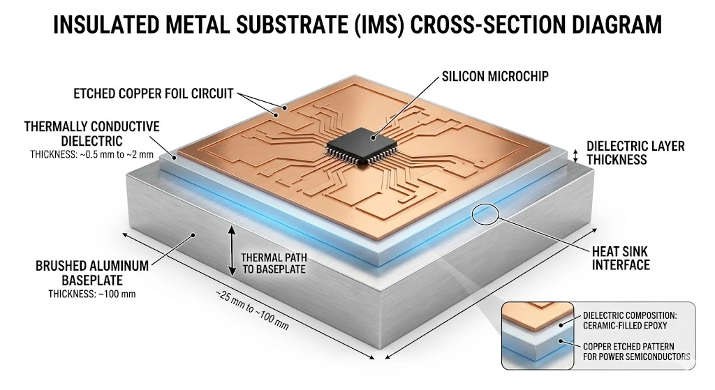
The Insulated Metal Substrate (IMS), frequently referred to in the industry as a Metal Core PCB (MCPCB), was engineered specifically to bridge the critical gap between necessary electrical isolation and mandatory thermal conductivity. It is universally recognized as the standard solution for high-power applications requiring significant heat dissipation within a compact, flat, planar form factor.
Deconstructing the “Sandwich” Architectural Structure
An IMS is fundamentally an engineered three-layer “sandwich” structure designed to drastically minimize the junction-to-case thermal resistance (Rth(j-c)) while maintaining strict high-voltage dielectric breakdown standards required for safety and operation. The three distinct functional layers are:
- The Metal Baseplate (Thermal Spreader): Forming the robust foundation of the IMS, this layer is typically constructed from aluminum (Al) or, in ultra-high-performance applications, copper (Cu). Aluminum is the dominant choice due to its optimal balance of low cost, lightweight properties, and excellent thermal conductivity (ranging from 150 to 230 W/m·K, depending on the specific alloy series). The baseplate acts as a primary thermal spreader, drawing concentrated heat away from the tiny semiconductor die and distributing it evenly over a much larger surface area before transferring it to the final external heatsink.
- The Dielectric Layer (The Thermal Highway): This is the most critical, proprietary, and technologically complex component of the IMS. It must provide robust electrical isolation (often requiring voltage breakdown ratings exceeding 3kV, 4kV, or even higher for industrial drives) while simultaneously conducting heat. Standard FR4 fails here. IMS dielectrics consist of a specialized epoxy resin matrix that is heavily filled with thermally conductive microscopic ceramic particles, such as Aluminum Oxide (Al2O3) or Aluminum Nitride (AlN). The exact blending and sizing of these ceramic particles dictate the overall thermal performance.
- The Copper Foil (The Circuit Layer): The top layer is a standard copper foil (typically ranging from 1 oz to heavy copper weights of 6 oz or more for high-current traction applications) that is chemically etched to form the specific electrical circuit traces, component pad layouts, and high-current mounting points.
Thermal Performance: Shattering the FR4 Barrier
The physical parameters of an IMS illustrate a dramatic leap in thermal management capability. Thanks to the highly engineered ceramic-filled dielectric layer, a standard IMS achieves a thermal conductivity ranging from 1.0 to 3.0 W/m·K, while premium advanced IMS materials can reach up to 8.0 W/m·K or higher. When compared directly to the traditional FR4 thermal conductivity of 0.25 W/m·K, the dielectric layer in an IMS offers a heat dissipation efficiency that is generally 5 times higher, and often an order of magnitude better in premium grades.
In practical hardware engineering terms, this physical reality means that heat generated by a surface-mounted power component travels via an ultra-short, highly efficient thermal path. The heat moves from the component package lead, directly through the heavy copper trace, traverses the highly conductive microscopic dielectric layer, and instantly spreads into the massive aluminum baseplate. This architecture fundamentally lowers the total thermal impedance of the system, keeping the operating Tj well within safe limits even under heavy electrical loads.
Typical Application Scenarios for IMS Technology
Because of its robust mechanical structure and exceptional planar thermal performance, IMS technology has become the definitive backbone for several key industrial sectors:
- Portable Welding Equipment: In portable inverter welders, power density is the primary design constraint. IMS boards allow high-current switching devices to operate safely within extremely confined physical spaces without the need for massive, heavy forced-air cooling tunnels, keeping the equipment truly portable.
- Solar Micro-Inverters: Typically installed directly beneath rooftop photovoltaic (PV) panels, micro-inverters face brutally harsh ambient temperatures and often experience zero forced airflow. IMS provides the highly efficient passive cooling required to maintain the reliability and prevent thermal degradation of the inverter’s power stage over a demanding 20-to-25-year operational lifespan.
- High-Brightness LED Lighting: Automotive headlamps and industrial high-bay lighting rely heavily on IMS to draw heat away from compact LED dies, preventing color shifting and lumen depreciation.
Double-Sided Cooling (DSC): The Automotive Traction Revolution
While IMS is highly effective for single-sided surface-mount designs and discrete module applications, the relentless push for massive electrification in the automotive sector—specifically the high-power traction inverters found in modern Electric Vehicles (EVs)—has aggressively exposed the physical limits of single-sided cooling architectures. To extract the absolute maximum performance from advanced silicon and SiC dies, packaging engineers engineered a revolutionary approach: Double-Sided Cooling (DSC) technology.
The Critical Limitations of Traditional Wirebonding
Traditional high-power semiconductor modules utilize a strictly single-sided cooling paradigm. The bare semiconductor die is soldered to a direct bonded copper (DBC) or active metal brazed (AMB) substrate, which in turn rests on a thick copper baseplate. Electrical connections to the top surface of the die (the emitter of an IGBT or the source of a MOSFET) are achieved using arrays of ultrasonic aluminum wirebonds. While standard practice for decades, this traditional architecture has two severe limitations in modern ultra-high-power density applications:
- Severe Thermal Asymmetry: In a wirebonded module, heat can only escape downwards through the bottom baseplate. The top of the die is covered entirely in wirebonds and encapsulating silicone gel. Because silicone gel and wirebonds are poor thermal conductors, the top side of the die offers practically zero thermal dissipation. The module relies entirely on one thermal pathway.
- Mechanical Fatigue and Electrical Vulnerability: Wirebonds physically introduce parasitic stray inductance. During high-frequency switching operations (especially with SiC devices), this inductance causes harmful voltage spikes (calculated by V = L × di/dt) that can exceed device ratings. Furthermore, continuous thermal cycling in EVs causes materials to expand and contract. Over time, this causes mechanical shear stress at the microscopic bond heels, eventually leading to wirebond lift-off or wirebond fracture—one of the most common and fatal failure modes in high-power traction inverters.
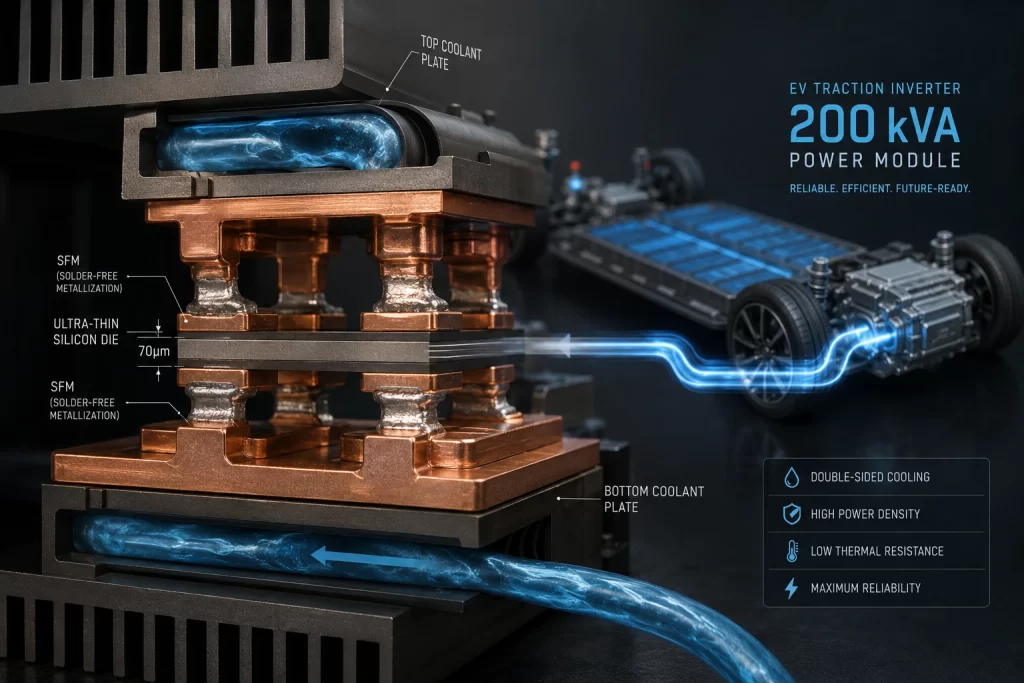
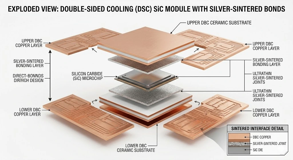
The DSC Architecture: Wirebond-less Packaging and Sintered Front Metal (SFM)
Double-Sided Cooling (DSC) technology fundamentally reimagines the power module by completely eliminating traditional aluminum wirebonds—a structural paradigm known as wirebond-less or planar packaging. Instead of delicate wires, the top surface of the semiconductor die is metallized and physically connected to a solid, highly thermally conductive top lead frame, copper clip, or spacer.
To achieve this robust top-side connection, engineers utilize advanced attachment technologies such as Sintered Front Metal (SFM). Silver (Ag) or Copper (Cu) sintering is a metallurgical process where microscopic metal particles are fused together under heat and pressure below their actual melting point. Sintering provides a solid metallurgical bond that boasts significantly higher thermal and electrical conductivity compared to traditional lead-free solders. Crucially, a sintered joint has a much higher melting point than standard solder, preventing the joint from remelting during extreme overload conditions. In a DSC module, the semiconductor die is essentially sandwiched tightly between two high-performance thermal substrates.
Amplifying Performance: Ampacity, Inductance, and Power Density
The introduction of the top cooling path changes the physics of the module. Heat now flows out of both the bottom and the top of the semiconductor die simultaneously. This dual-path parallel thermal resistance network dramatically lowers the total system Rth(j-c).
By effectively doubling the active cooling surface area, DSC enables a massive increase in continuous power density. Empirical engineering data demonstrates that, for a given physical die size and a strict maximum junction temperature limit, DSC technology allows the current carrying capacity (often referred to as ampacity) to increase by a staggering 30% compared to structurally equivalent single-sided cooling modules. This 30% performance boost allows automotive powertrain engineers to either increase the total power output and acceleration of an EV traction inverter without increasing its physical size, or significantly shrink the physical footprint and weight of the inverter while maintaining the original power output.
Furthermore, replacing thin, looping aluminum wirebonds with broad, solid copper spacers or planar lead frames severely slashes the internal stray inductance of the module. This reduction in parasitic inductance is absolutely critical for the safe and efficient operation of ultra-fast switching WBG devices. Lower inductance minimizes dangerous switching voltage overshoots, reduces electromagnetic interference (EMI), and allows the devices to switch faster, thereby minimizing switching losses and improving total vehicle range.
Engineering Selection Guide: Navigating Thermo-Mechanical Challenges
Deciding between a cost-effective IMS architecture and a high-performance DSC module depends heavily on the specific application’s power density requirements, volumetric constraints, and commercial cost budget. Understanding voltage, current, and thermal management is the core trio of IGBT and module selection. However, regardless of the chosen technology, hardware engineers must rigorously address internal thermo-mechanical stresses and the physical interfaces between external components.
Mitigating Coefficient of Thermal Expansion (CTE) Mismatch
Power electronics operate in a highly dynamic, aggressive thermal environment. As electrical load currents fluctuate based on system demand, internal temperatures rise and fall rapidly, causing all internal materials to expand and contract. This introduces the critical engineering concept of the Coefficient of Thermal Expansion (CTE), measured in parts per million per Kelvin (ppm/K).
Different materials within a power assembly expand at vastly different rates when heated:
- Silicon (Si) Die: Approximately 3 ppm/K
- Silicon Carbide (SiC) Die: Approximately 4 ppm/K
- Copper (Cu): Approximately 17 ppm/K
- Aluminum (Al): Approximately 23 ppm/K
In both IMS assemblies and DSC modules, materials with drastically divergent CTEs are permanently bonded together. When the entire system undergoes active thermal cycling (ΔT), the uneven expansion rates create severe mechanical shear stress on the solder layers, sintered joints, and dielectrics connecting the layers. Over tens of thousands of operating cycles, this relentless mechanical fatigue leads to material delamination, solder layer cracking, void propagation, and ultimate catastrophic device failure.
When engineering with IMS, designers must evaluate whether the chosen dielectric layer possesses enough inherent elasticity (a lower Young’s Modulus) to absorb the massive shear stress generated between the highly expansive aluminum baseplate and the lower-expanding copper traces and silicon components. In high-end DSC modules, advanced buffer materials and specialized copper spacer designs are heavily engineered specifically to mitigate the extreme CTE mismatch between the rigid, brittle silicon/SiC die and the massive, highly expansive copper cooling plates.
Mastering Thermal Interface Materials (TIM) for System Reliability
Even the most advanced, expensive IMS board or DSC module is entirely rendered useless if the generated heat cannot effectively transfer from the module’s exterior case to the final liquid-cooled cold plate or extruded finned heatsink. Due to microscopic surface roughness (asperities) on all machined metal surfaces, when two flat plates are bolted together, the actual metal-to-metal contact area can be alarmingly low—often between 5% to 10%. The remaining 90% of the interface consists of microscopic air pockets. Because air is a profound thermal insulator, these gaps cause temperatures to spike.
Thermal Interface Materials (TIM) are explicitly used to displace this insulating air and create a continuous conductive thermal path. To achieve reliability, engineers must carefully match the physical properties of the TIM to the application’s demands, keeping in mind that mastering thermal management and Rth is deeply dependent on proper heatsink and interface design.
| TIM Category | Physical Characteristics & Mechanism | Typical Engineering Application | Selection Precautions & Failure Modes |
|---|---|---|---|
| Standard Thermal Grease (Paste) | Low cost, highly viscous liquid base loaded with conductive particles. Excellent gap filling and very low initial thermal resistance. | General purpose industrial inverters, standard IMS board mounting, commercial power supplies. | Highly prone to the “pump-out” effect over time. Repeated thermal cycling physically squeezes the grease out of the interface, leading to voiding, massive thermal degradation, and eventual failure. |
| Phase Change Materials (PCM) | Solid at room temperature for easy handling. Melts at a specific operating temperature (e.g., 50°C to 60°C) to flow and perfectly fill micro-voids like grease. | Automotive EV traction inverters, high-reliability industrial drives, renewable energy converters. | Effectively eliminates pump-out issues. However, it requires precise application thickness and specific mounting pressure to ensure optimal phase transition performance and minimum bond line thickness. |
| Graphite Thermal Pads | Highly anisotropic material (excellent lateral heat spreading, moderate vertical conductivity). Solid state, completely immune to pump-out or drying. | High-temperature WBG (SiC/GaN) applications, military, and aerospace systems. | Requires extremely high, consistent mechanical clamping force to achieve low thermal resistance. Furthermore, graphite is highly electrically conductive; extreme care must be taken to ensure it does not short out electrical pins. |
Hardware engineers must accurately calculate the total thermal stack-up resistance. Selecting an advanced PCM over a standard silicone-based grease can prevent long-term mechanical fatigue and thermal degradation at the critical interface, ensuring the case-to-heatsink thermal resistance (Rth(c-s)) remains exceptionally stable over the product’s entire 10-to-20-year operational lifespan.
Conclusion: The Future of High-Density Thermal Integration
The continuous evolution from standard FR4 printed circuit boards to engineered Insulated Metal Substrates (IMS) and advanced Double-Sided Cooling (DSC) packages demonstrates the power electronics industry’s unwavering commitment to overcoming thermal bottlenecks. By utilizing a highly engineered ceramic-filled dielectric layer, IMS technology provides a simple, highly manufacturable, yet incredibly powerful 5x enhancement in planar heat dissipation. It rightfully serves as the robust, cost-effective backbone for high-density portable power systems and distributed renewable energy installations.
Conversely, Double-Sided Cooling (DSC) represents the absolute bleeding edge of high-power density packaging. By ruthlessly eliminating vulnerable wirebonds and introducing sintered front metals to create parallel top-and-bottom thermal pathways, DSC unlocks a transformative 30% increase in current carrying capacity. This technology is actively fueling the modern Electric Vehicle revolution, allowing inverters to handle massive power surges in smaller footprints.
As the industry accelerates toward higher adoption rates of SiC and GaN technologies, the high switching frequencies and localized heat fluxes will continue to challenge traditional limits. For the modern hardware engineer, long-term product reliability lies in understanding the deep physics behind these advanced thermal technologies, meticulously matching CTE profiles to prevent mechanical fatigue, and rigorously selecting the optimal TIM to ensure that superior electrical performance is never throttled by thermal constraints.
Featured Solutions: High-Performance Modules for Demanding Thermal Environments
To implement the advanced thermal management architectures discussed above, selecting the optimal power module is critical. Based on the engineering challenges of CTE mismatch, interface thermal resistance, and parasitic inductance, the Shunlongwei Technical Team recommends evaluating the following industry-leading platforms:
- Infineon PrimePACK™ FF Series (e.g., FF1400R17IP4):
Designed to handle massive power cycling, these large-footprint dual modules offer exceptional CTE stress mitigation. They are highly optimized for use with advanced Phase Change Materials (PCM) to eliminate thermal grease pump-out in extreme environments. - Infineon EconoDUAL™ FF Series (e.g., FF600R12ME4):
The definitive industry standard for single-sided planar heat dissipation. These modules integrate perfectly with robust Insulated Metal Substrate (IMS) cooling solutions, making them the workhorse for commercial solar inverters and industrial motor drives.
For detailed datasheets, thermal stack-up guidelines, or specialized procurement inquiries, please contact our engineering support team.
Content in This Series
Mastering SMD IGBTs on IMS: A Guide to High-Density Welding Power Supplies