The industrial power electronics landscape is changing. For decades, the priority was simply raw power. Today, engineers are tasked with a more complex challenge: delivering that same power in smaller, lighter, and more efficient packages. This shift is particularly obvious in the design of portable welding machines.
Modern welding power supplies are moving away from traditional, heavy line-frequency transformers. Instead, they utilize high-frequency inverter topologies. By switching at frequencies of 30 kHz or higher, engineers can drastically shrink the size of magnetic components and filter capacitors. However, this high-frequency operation places immense stress on the power semiconductor switches, specifically the Insulated Gate Bipolar Transistors (IGBTs).
To meet these extreme demands, the power electronics industry is undergoing a massive shift in assembly. We are finally leaving behind outdated, hand-soldered through-hole components.
Instead, engineers are embracing Surface-Mount Technology (SMT). By mounting compact SMD packages directly onto an Insulated Metal Substrate (IMS), we can fundamentally push the size and thermal limits of modern welding converters.
This article explores the technical advantages of using D2Pak IGBTs on IMS for welding applications. We will break down how this architecture solves parasitic inductance issues, improves thermal management, and how to conquer the specific manufacturing challenges associated with IMS reflow soldering.
The Problem with Traditional Through-Hole Designs
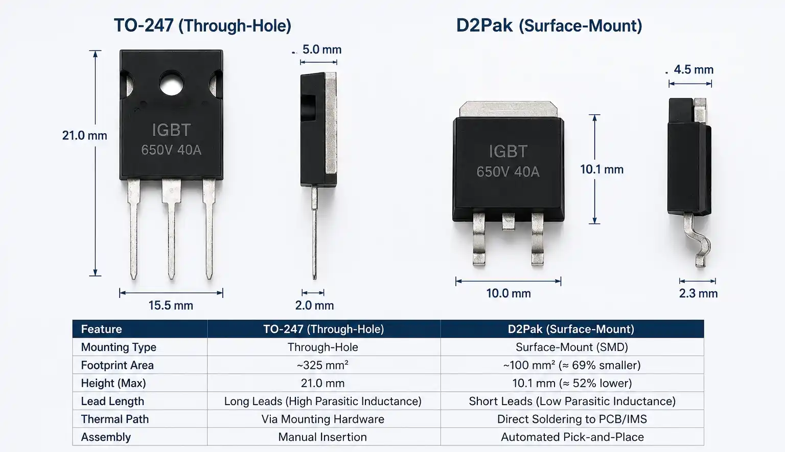
For a long time, the TO-247 package was the undisputed king of high-power discrete IGBTs. It is robust, can handle high currents, and is relatively easy to bolt onto a large aluminum heatsink. But as the demand for portable, lightweight welding machines grows, the limitations of the TO-247 become glaringly obvious.
Labor-Intensive Assembly: Through-hole components generally require manual insertion into the Printed Circuit Board (PCB). Workers must manually bend the leads, apply thermal grease or silicone pads, and physically screw the device to a heatsink. In an era of rising labor costs, this manual process is expensive and prone to human error.
Parasitic Inductance: The long, extending metallic leads of a TO-247 package act as tiny inductors. In low-frequency applications, this is negligible. But when switching at 40 kHz, these parasitic elements become a serious threat to system stability.
To truly understand how device packaging affects overall converter design, it is highly recommended to review The Engineer’s Ultimate Guide: An In-Depth Analysis of IGBT Modules, which provides foundational knowledge on power semiconductor architectures.
The Solution: Surface-Mounted Devices (SMD)
The logical step forward is automated assembly using Surface-Mounted Devices. Devices like the D2Pak (TO-263-3) can be placed onto a circuit board using high-speed pick-and-place machines, entirely eliminating manual insertion.
Historically, SMD packages were considered too small to handle the massive currents required for welding. However, advancements in ultra-thin silicon wafer technology—such as the 650 V TRENCHSTOP™ 5 IGBT—now allow for incredibly high power densities within these compact footprints. For example, modern D2Pak co-pack devices can comfortably handle 40 A of current, making them a direct replacement for bulky TO-247 devices in 4 kW half-bridge welding converters.
What is an Insulated Metal Substrate (IMS)?
But there is a major catch. You cannot simply solder a 40 A high-power semiconductor onto a standard FR4 fiberglass Printed Circuit Board (PCB).
Standard FR4 material is a terrible thermal conductor. If you attempt this, the IGBT will trap its own heat and burn out within seconds. To safely utilize SMD packages in high-power converters, you must upgrade to an Insulated Metal Substrate (IMS).
An IMS is a specialized type of circuit board engineered specifically for superior thermal extraction. It consists of three critical layers:
- The Metal Base Plate: This is the thickest part of the board, usually made of aluminum (typically 1.6 mm thick). It provides mechanical rigidity and acts as the primary heat spreader, pulling heat away from the components and transferring it to the external heatsink.
- The Dielectric Layer: This is the “secret sauce” of the IMS. It is an ultra-thin (approx. 100 μm) polymer-ceramic layer. It must provide robust electrical isolation (often withstanding over 2.5 kVRMS) while maintaining an extremely low thermal resistance to allow heat to pass through freely.
- The Copper Circuit Foil: The top layer where the actual electronic tracks are etched. Heavy copper (e.g., 3 oz/ft2) is used to carry high welding currents without generating excessive resistive heating.
By soldering the D2Pak directly onto the copper foil of the IMS, the heat generated by the semiconductor die has a direct, incredibly short path to the aluminum baseplate.
For a deeper dive into managing junction temperatures and heat dissipation strategies, explore this comprehensive guide: Mastering IGBT Thermal Management: A Guide to Packaging, Rth, and Heatsink Design.
Winning the Battle Against Stray Inductance
While the thermal benefits of IMS are excellent, the electrical benefits are arguably even more important for system reliability.
In power electronics, stray inductance (Lstray) is the parasitic inductance naturally present in the PCB traces and the component packages themselves. When an IGBT turns off, it interrupts a large flow of current very quickly. According to the laws of physics, a rapid change in current (di/dt) across an inductor generates a voltage spike.
If this voltage spike—seen across the collector-emitter terminals (VCE)—exceeds the rated breakdown voltage of the IGBT, the silicon die will be destroyed instantly.
D2Pak vs. TO-247: The Numbers
Because the TO-247 package has long wire leads, it inherently possesses a higher stray inductance. A typical TO-247 layout might have a package stray inductance of around 15 nH.
In contrast, the D2Pak sits flat against the board with virtually zero lead length. The total stray inductance for a D2Pak layout can be as low as 5 nH. This represents a massive 66% reduction in parasitic inductance.
The Result: The D2Pak on IMS experiences significantly lower turn-off voltage overshoots. This gives engineers a wider safety margin, increases the lifespan of the machine, and allows for the use of smaller gate resistors (RG), which further reduces switching power losses.
To learn more about optimizing circuit layouts to reduce voltage spikes, read Minimizing Stray Inductance in Traction Converters: A Physical Path to High Power Density.
The Core Challenge: Mastering the Reflow Soldering Process
The electrical and thermal advantages of the SMD-on-IMS architecture are undeniable. However, actually manufacturing these boards presents a unique and frustrating challenge for production engineers: the reflow soldering process.
To avoid catastrophic solder failures, you must completely rewrite your oven’s thermal profile.
Based on extensive metallurgical testing and guidelines from major IGBT manufacturers, a successful D2Pak-on-IMS reflow requires precise control over five distinct stages:
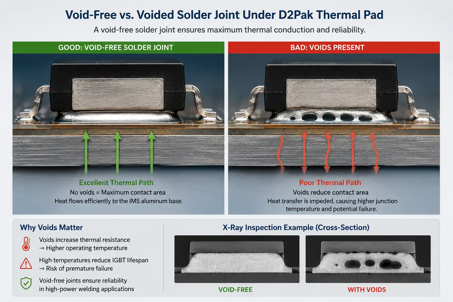
An IMS board, however, is a giant block of aluminum. It possesses a massive thermal mass. If you put an IMS board into a reflow oven using a standard FR4 temperature profile, the aluminum baseplate acts like a giant heatsink. It absorbs all the heat, preventing the solder paste from ever reaching its liquidus temperature.
The result? “Cold” solder joints, poor wetting, and large air voids trapped underneath the IGBT. These voids ruin the thermal conductivity, causing the IGBT to overheat and fail in the field.
Optimizing the IMS Reflow Profile
To successfully solder a D2Pak to an IMS, the reflow oven’s thermal profile must be completely rewritten to account for the heavy thermal mass. Based on extensive metallurgical testing and semiconductor guidelines, a proper IMS reflow profile requires precise control over five stages:
- Ramp-Up Phase (1 to 3 °C/s): The board is heated gently. If heated too fast, the solvents in the solder paste will boil violently, causing solder beads to splatter across the board.
- The Critical Preheating / Soak Zone (Approx. 90 seconds): This is where standard profiles fail. The board must sit in a specific temperature range (usually 150 °C to 200 °C) for an extended period. This allows the massive aluminum baseplate time to absorb heat and reach a uniform temperature across the entire board, without prematurely burning off the flux.
- Reflow Time (Approx. 55 seconds): The temperature is pushed above the melting point of the solder alloy (liquidus). This window gives the solder enough time to melt completely, flow outward, and wet both the circuit board copper and the IGBT’s thermal tab.
- Peak Temperature (Target: 244 °C): The highest temperature reached. It must be hot enough to guarantee total solder melting, but kept strictly below the point where the IMS dielectric layer or the semiconductor casing begins to degrade.
- Ramp-Down Phase (2 to 4 °C/s): The board must be cooled in a controlled manner. Cooling too slowly creates brittle, oversized crystalline structures in the solder. Cooling too rapidly introduces severe mechanical stress that can crack the solder joint.
For more foundational knowledge on how these semiconductor devices operate at a physics level, you can reference the basic operating principles outlined on the Wikipedia page for Insulated-gate bipolar transistors.
Real-World Validation: Thermal and Electrical Wins
Theory is excellent, but industrial engineering requires empirical proof. To validate the SMD-on-IMS architecture, engineers constructed two identical 4 kW half-bridge welding power supplies.
- System A: Utilized traditional TO-247 packages bolted to a heatsink with a standard silicone thermal pad.
- System B: Utilized the new D2Pak packages reflow-soldered onto an IMS, which was then attached to the exact same heatsink.
Both systems were run at a strenuous 60% welding duty cycle (6 minutes ON, 4 minutes OFF) delivering 160 ADC at a 35 kHz switching frequency.
The Results Speak for Themselves
Thermal Performance: The D2Pak-on-IMS solution ran significantly cooler. The case temperature of the traditional TO-247 system ran between 4 °C and 7 °C hotter than the IMS system, depending on the quality of the thermal pad used. In power electronics, lowering the operating temperature by 7 degrees drastically increases the overall lifespan and reliability of the silicon die.
Electrical Performance: Just as the physics predicted, the reduced stray inductance of the D2Pak (5 nH vs 15 nH) fundamentally changed the switching behavior. Oscilloscope measurements confirmed that the D2Pak system exhibited a much smaller VCE voltage overshoot during turn-off. The aggressive “ringing” seen in the TO-247 system was heavily damped in the IMS layout.
Conclusion: The Future of High-Frequency Assembly
The demand for portable, high-performance welding machines—and similar equipment like EV chargers and solar inverters—will only continue to grow. Manufacturers can no longer afford to rely on bulky components and manual labor.
The transition from through-hole TO-247 discrete devices to SMD D2Pak devices mounted on Insulated Metal Substrates represents a massive leap forward in power converter design.
By embracing this architecture, engineers achieve a trifecta of benefits:
- Automated Manufacturing: Lowering labor costs and improving assembly consistency.
- Superior Thermals: Utilizing IMS to pull heat directly away from the die, extending component life.
- Enhanced Electrical Stability: Minimizing parasitic inductance to tame destructive voltage spikes and enable higher switching frequencies.
While the manufacturing challenge of dialing in the perfect IMS reflow profile is real, the blueprint for success is clear. For engineering teams willing to optimize their thermal processes, the SMD-on-IMS architecture provides a definitive competitive advantage in the modern power electronics market.
Featured Power Modules for High-Frequency Welding Converters
Infineon FF300R12ME4 EconoDUAL™ IGBT Module
A widely used 1200 V / 300 A EconoDUAL module suitable for welding power supplies, UPS systems, and industrial inverter platforms.
SEMIKRON SKM200GB12T4 SEMITRANS® 3 IGBT Module
This 1200 V SEMITRANS® module is commonly seen in industrial motor drives and inverter-based welding equipment.
For datasheets or module selection support, please contact the Shunlongwei engineering team.