Precision Gate Drive Design: Mastering Gate Charge (QG) and Miller Effect Mitigation Strategies
In high-power electronics design, the gate drive circuit represents the critical “last mile” that dictates the dynamic performance, efficiency, thermal stability, and overall reliability of modern semiconductor switches. Whether designing with silicon Power MOSFETs, Insulated Gate Bipolar Transistors (IGBTs), or Wide Bandgap (WBG) devices such as Silicon Carbide (SiC) MOSFETs, engineers frequently face a frustrating dilemma: circuit simulations look promising, yet hardware prototypes suffer from excessive switching losses, electromagnetic interference (EMI) ringing, or catastrophic shoot-through failures.
A primary root cause of these issues is a flawed approach to gate drive sizing—specifically, relying on static input capacitance specifications (Ciss) found on component datasheets rather than evaluating dynamic Gate Charge (QG) metrics. Furthermore, failing to account for the non-linear behavior of the Miller capacitance (Cgd or Cgc) during high dV/dt transitions leaves power stages vulnerable to parasitic turn-on.
This technical guide provides hardware design engineers with an in-depth analytical framework for gate drive design. We examine the physics behind the gate charge characteristic curve, demystify the Miller Plateau phenomenon, establish precise mathematical models for gate driver power and peak current requirements, and present validated circuit strategies to suppress Miller-induced parasitic turn-on.
The Static Capacitance Fallacy: Why Ciss Belongs in Small-Signal Physics
Historically, novice engineers attempted to calculate required gate drive currents using standard capacitance equations based on input capacitance (Ciss). On power transistor datasheets, terminal capacitances are typically defined as:
- Input Capacitance: Ciss = Cgs + Cgd (for MOSFETs) or Cies = Cge + Cgc (for IGBTs)
- Output Capacitance: Coss = Cds + Cgd
- Reverse Transfer Capacitance: Crss = Cgd (also referred to as Miller capacitance)
The fundamental trap of using Ciss for gate driver dimensioning lies in how datasheet capacitance values are measured. Datasheet parameters for Ciss, Coss, and Crss are static, small-signal AC measurements obtained at a fixed drain-to-source voltage (e.g., VDS = 25V or 800V) with a small 1 MHz test signal applied. However, during a hard-switching power transition, the drain-to-source voltage is far from static—it swings across the full DC bus voltage range.
Internal semiconductor depletion regions vary dynamically with applied bias voltage. As VDS collapses toward zero during device turn-on, the physical thickness of the depletion layer shrinks dramatically. Consequently, the reverse transfer capacitance Cgd increases non-linearly by up to two to three orders of magnitude. A small-signal Ciss value completely ignores this massive surge in effective capacitance. Sizing a gate driver based solely on Ciss invariably results in an under-designed driver stage incapable of delivering sufficient peak current during switching transitions.
For a detailed analysis on how parasitic capacitance dynamics influence overall silicon losses and switching behaviors, review our comprehensive technical article on Power MOSFET Deep Dive: The Engineer’s Guide to Selection, Losses, and Thermal Design.
Deconstructing the Gate Charge (QG) Curve and the Miller Plateau
To overcome the limitations of static capacitance values, semiconductor manufacturers provide the Gate Charge (QG) characteristic curve. Gate charge represents the actual total electric charge (measured in nanoCoulombs, nC) that the driver circuit must inject into or extract from the gate terminal to transition the semiconductor switch between its OFF and ON states under specified operating voltage and drain current conditions.
Evaluating a standard VGS versus QG curve reveals four distinct operational phases during a hard-switching turn-on event:
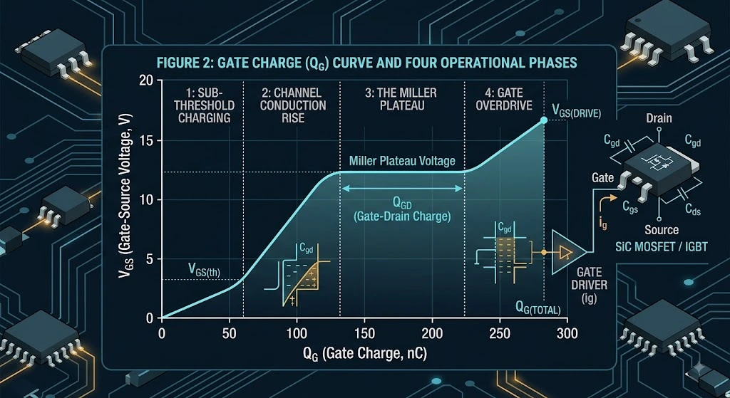
Phase 1: Sub-Threshold Charging (0 to Qgs1)
When the gate driver turns on, it sources current into the gate terminal. During this initial phase, the gate-to-source voltage VGS rises linearly from 0V (or a negative turn-off bias) up to the device threshold voltage VGS(th). The gate current charges the static gate-to-source capacitance Cgs. The main power channel remains non-conductive, and zero load current flows through the device.
Phase 2: Channel Conduction & Load Current Rise (Qgs1 to Qgs)
Once VGS crosses VGS(th), the semiconductor channel begins to form. Drain current ID rises rapidly from zero to full load current, dictated by the transconductance (gfs) of the switch. During this interval, VGS continues to rise until it reaches the Miller Plateau Voltage level, designated as Vplat. The drain-to-source voltage VDS remains clamped at the full DC bus voltage level because the freewheeling diode in the circuit has not yet completely turned off. This overlapping period of maximum voltage and rising current represents a substantial portion of device turn-on energy loss (Eon).
Phase 3: The Miller Plateau Region (Qgs to Qgs + Qgd)
The Miller Plateau represents the most critical phase of the power switching cycle. During this interval, the gate-to-source voltage VGS completely stops rising and remains clamped at a flat, constant voltage level (Vplat). Engineers unfamiliar with power semiconductor physics often incorrectly assume the gate driver has failed during this plateau.
In reality, as the load current reaches its maximum, the drain-to-source voltage VDS begins its rapid fall toward the low on-state conduction voltage VDS(on). The rapid rate of change of voltage over time (dVDS/dt) forces a displacement current to flow out of the reverse transfer capacitance (Cgd). Because VGS is pinned at Vplat, 100% of the current supplied by the gate driver IC is redirected to discharge the rapidly expanding Cgd capacitance. The length of time the device spends in the Miller Plateau (tplat) is directly proportional to the total gate-to-drain charge (Qgd) and inversely proportional to the gate driver current (IG):
tplat = Qgd / IG
Minimizing this duration is vital because VDS and ID simultaneously exist at high levels throughout Phase 3, generating the vast majority of hard-switching power losses.
Phase 4: Gate Overdrive / Channel Saturation (Qgs + Qgd to QG)
After VDS drops to its fully saturated minimum on-state level, the displacement current through Cgd drops to zero. Gate current once again charges Cgs and Cgd in parallel, causing VGS to rise from Vplat to the final driver output rail voltage (e.g., +15V or +18V). Driving VGS fully to the specified driver rail voltage ensures the channel achieves minimum on-resistance (RDS(on) or VCE(sat)), suppressing conduction losses.
Quantitative Gate Driver Sizing: Mathematical Calculations
To design an accurate and robust gate driver stage, hardware engineers must calculate two key parameters: average power supply output requirements and peak sourcing/sinking current limits.
1. Calculating Average Gate Drive Power
Every switching cycle requires injecting a discrete quantity of charge (QG) into the gate network during turn-on and extracting it during turn-off. The total average power (PDRV) required from the gate drive power supply is calculated using the total gate charge, total gate voltage swing (ΔVGS), and operating switching frequency (fsw):
PDRV = QG × ΔVGS × fsw
Where:
- QG: Total gate charge at the specified driver supply voltage (Coulombs).
- ΔVGS: Total gate voltage swing, defined as VDRV,pos – VDRV,neg (Volts).
- fsw: Operating switching frequency (Hertz).
Practical Calculation Example:
Consider a high-frequency solar inverter design operating an IGBT switch with a total gate charge QG = 220 nC, driven by a dual-rail gate driver with VDRV,pos = +15V and VDRV,neg = -5V (ΔVGS = 20V) operating at fsw = 80 kHz:
PDRV = (220 × 10-9 C) × (20 V) × (80,000 Hz) = 0.352 Watts
To ensure long-term thermal reliability and account for internal driver stage dissipation and parasitic series resistance, engineers should apply a minimum 30% engineering design margin, selecting a bias supply rated for at least 0.46 Watts per gate channel.
For additional details regarding parameter trade-offs when selecting power transistors for elevated frequencies, refer to our specialized guide on IGBT Selection Beyond VCE(sat): A Guide for High-Frequency Designs.
2. Calculating Peak Gate Sourcing and Sinking Currents
To ensure fast transition times through the Miller Plateau without exceeding the maximum current limits of the gate driver IC, engineers must calculate the maximum peak sourcing (turn-on) and sinking (turn-off) currents. Peak current is limited by the total loop resistance, which comprises the driver IC internal output resistance, external gate resistor (RG,ext), and device internal gate resistance (RG,int):
IPK,src = (VDRV,pos – Vplat) / (RDRV,hi + RG,ext,on + RG,int)
IPK,snk = (Vplat – VDRV,neg) / (RDRV,lo + RG,ext,off + RG,int)
For comprehensive equations detailing gate loop impedance design and parasitic damping calculations, consult Texas Instruments’ landmark reference manual, Fundamentals of MOSFET and IGBT Gate Driver Circuits (SLUA618).
Understanding Parasitic Turn-On (PTO) and dv/dt Induced Spikes
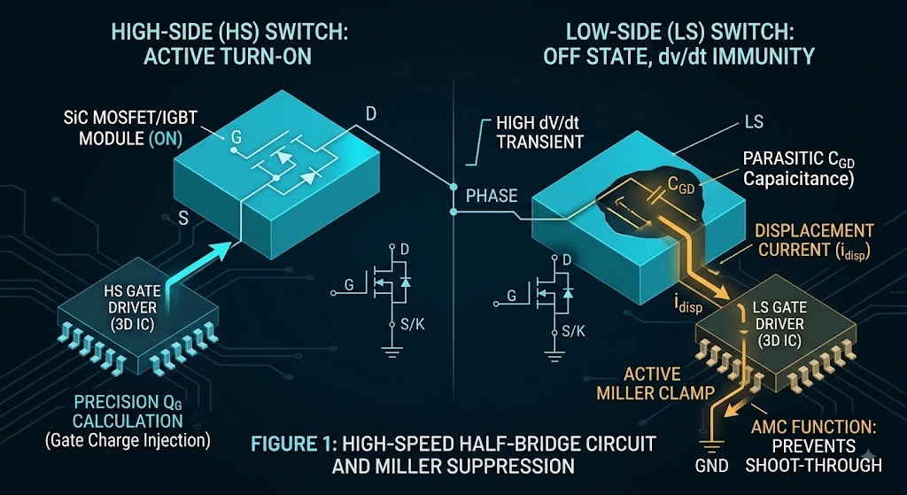
While optimizing gate drive current speeds up switching transitions, high switching speeds introduce a severe secondary phenomenon known as Parasitic Turn-On (PTO), or dv/dt-induced cross-conduction. PTO is particularly prevalent in bridge topologies (half-bridge, full-bridge, and three-phase motor drives) featuring a high-side and low-side switch pair connected across a common DC link voltage bus.
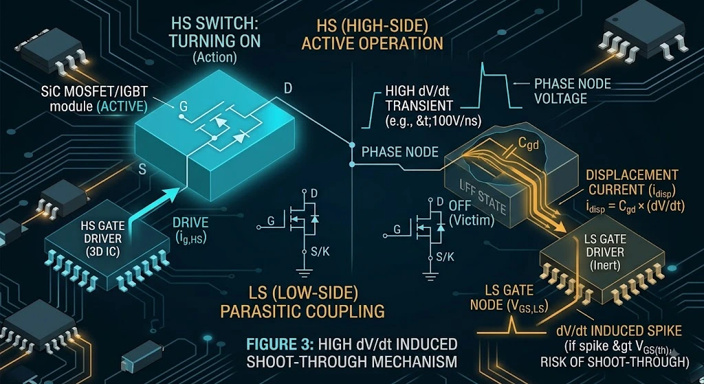
Consider a half-bridge stage where the low-side switch is held in the OFF state while the high-side switch actively turns ON. As the high-side switch conducts, the voltage across the low-side switch rises extremely rapidly from zero up to the full DC bus voltage level (high positive dVDS/dt or dVCE/dt).
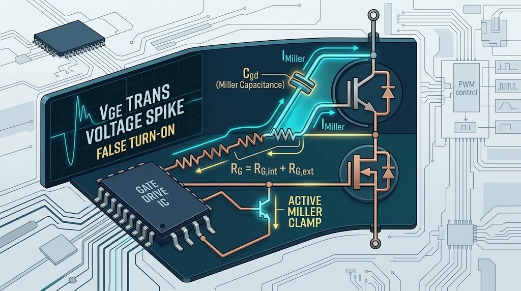
This high dv/dt transient forces a capacitive displacement current (idisp) to flow through the low-side switch’s internal Miller capacitance (Cgd):
idisp = Cgd × (dVDS / dt)
This displacement current enters the gate node of the off-state device and must flow back to ground through the off-state gate resistor network and driver sinking output transistor. According to Ohm’s Law, this displacement current generates an induced voltage spike at the gate terminal (VGS,spike):
VGS,spike = idisp × (RG,ext,off + RG,int + RDRV,snk) = Cgd × (dVDS / dt) × RG,tot,off
If VGS,spike exceeds the gate threshold voltage VGS(th) of the off-state power switch, the device unintentionally turns back ON while the high-side switch is fully conducting. This creates a direct low-impedance short-circuit across the DC rail—a catastrophic scenario known as a “shoot-through” condition. Shoot-through events cause extreme current spikes, intense instantaneous thermal dissipation, severe EMI generation, and eventual failure of the power stage.
Wide Bandgap devices like Silicon Carbide (SiC) MOSFETs are especially sensitive to PTO because of their ultra-fast switching speed capability (dv/dt exceeding 50 to 100 V/ns) combined with relatively low threshold voltages (VGS(th) often drops below 2.0V at elevated operating temperatures). For an in-depth breakdown of wide-bandgap threshold behavior, examine our technical report on Mitigating Parasitic Turn-On (PTO) in SiC MOSFETs: The Critical Role of Miller Capacitance and Threshold Voltage Optimization.
Engineering Mitigation Strategies for Miller Effect Suppression
To eliminate parasitic turn-on without compromising turn-on switching speed and converter efficiency, hardware designers utilize four primary engineering mitigation strategies.
Strategy 1: Asymmetric Gate Resistors (Split Turn-On / Turn-Off Paths)
Using a single symmetrical gate resistor forces a compromise between turn-on dv/dt control and turn-off Miller immunity. Sizing a large gate resistor slows turn-on dv/dt to suppress EMI, but it simultaneously increases total off-state gate loop impedance (RG,tot,off), making the device vulnerable to dv/dt-induced gate voltage spikes.
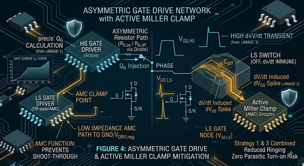
An asymmetric gate drive circuit decouples the turn-on and turn-off impedance paths by introducing a fast anti-parallel Schottky diode in series with a dedicated turn-off resistor (RG,off). This enables designers to select a larger RG,on to reduce switching noise while keeping RG,off minimal to provide a low-impedance path for Miller displacement currents during turn-off.
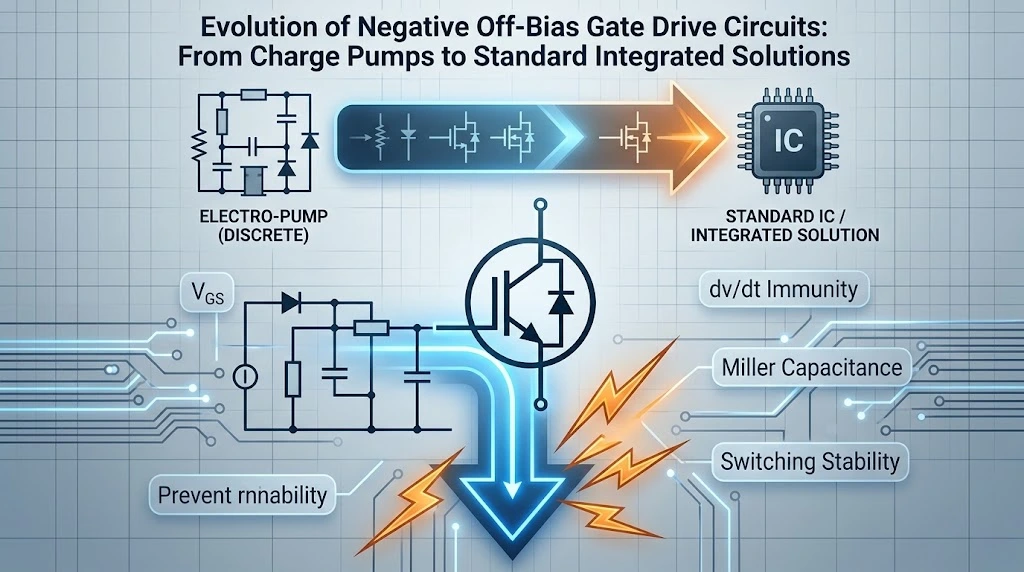
Strategy 2: Negative Off-State Bias Voltage (-VGS)
Applying a negative bias voltage (e.g., -3V to -5V for SiC MOSFETs; -8V to -15V for high-power IGBTs) during the off-state significantly increases the safety margin against parasitic turn-on. When a negative off-state bias is present, the induced gate voltage spike must overcome both the negative bias voltage and the device threshold voltage before channel conduction occurs:
Vmargin = |VDRV,neg| + VGS(th)
While negative bias is highly effective, it increases system complexity by requiring split-rail isolated power supplies or dedicated charge pump circuits.
Strategy 3: Active Miller Clamp (AMC)
An Active Miller Clamp provides an elegant hardware solution that eliminates the need for complex negative power supply rails in many low-to-medium power applications. Gate driver ICs with integrated AMC feature an auxiliary monitoring pin (CLAMP) connected directly to the power switch gate node downstream of the external turn-off resistor.
AMC Operational Sequence:
- When the driver initiates turn-off, current flows through the standard turn-off resistor RG,off.
- The driver monitors the falling gate voltage. Once VGS drops below a predefined internal threshold (typically 2.0V relative to ground or negative rail), the internal AMC logic activates a low-impedance internal N-channel MOSFET switch.
- The AMC switch shorts the gate node directly to ground (or negative supply), bypassing RG,off entirely.
- Because the Miller displacement current now flows through a sub-1-ohm path directly to ground, the induced gate voltage spike remains comfortably below VGS(th), preventing parasitic turn-on.
Strategy 4: PCB Layout Optimization & Kelvin Source Connections
Even the most advanced gate driver IC cannot overcome poor PCB layout parasitics. Parasitic loop inductance in the gate trace (LG) acts as a high-impedance choke against high-frequency dv/dt displacement currents, elevating the effective gate impedance during switching events.
Key PCB routing best practices include:
- Kelvin Source / Emitter Connections: Route the gate driver ground return trace directly to the dedicated Kelvin source/emitter pin of the switch package. This prevents heavy power loop di/dt current drops across package lead inductances from coupling into the sensitive gate control loop.
- Minimized Loop Area: Overlap the gate feed trace and Kelvin return trace on adjacent PCB inner layers to achieve magnetic field cancellation and minimize parasitic gate loop inductance.
- Proximity: Place the gate driver IC, decoupling capacitors, and Active Miller Clamp components as close as physically possible to the power semiconductor terminals.
For an expanded list of hardware assembly and board layout practices, consult our engineering guide, 5 Practical Tips for Robust IGBT Gate Drive Design to Prevent Catastrophic Failure.
Detailed recommendations regarding external gate resistor sizing and parasitic damping tuning are also provided in Texas Instruments’ application report, External Gate Resistor Design Guide for Gate Drivers (SLLA385).
Comparative Analysis of Miller Suppression Techniques
To assist power design engineers in selecting the optimal mitigation approach for specific system constraints, the following table compares the primary Miller effect suppression strategies:
| Suppression Technique | Primary Mechanism | System Complexity & Cost | Impact on Switching Losses | Recommended Application Scope |
|---|---|---|---|---|
| Asymmetric Gate Drive | Decouples turn-on and turn-off gate resistance via parallel diode. | Very Low (1 small signal diode + 1 resistor). | Negligible impact on turn-off losses. | Standard Si MOSFETs, low-power IGBTs. |
| Negative Gate Bias (-VGS) | Expands threshold voltage safety margin below ground. | Moderate to High (Requires negative supply rail). | Reduces turn-off energy loss (Eoff). | High-power IGBT modules, medium-to-high power SiC MOSFETs. |
| Active Miller Clamp (AMC) | Clamps gate node directly to ground via low-impedance switch during off-state. | Low to Moderate (Requires AMC-capable driver IC). | Zero efficiency penalty; optimizes turn-off speed. | High-speed SiC MOSFETs, compact EV chargers, industrial motor drives. |
| Kelvin Source Connection | Isolates power channel di/dt from gate signal return path. | Low (Requires 4-lead package and careful PCB routing). | Significantly reduces switching losses and ringing. | Mandatory for all WBG (SiC/GaN) and high-current IGBT designs. |
Engineering Validation & Bench Testing Checklist
When prototyping high-power converter designs, engineering teams should execute a systematic bench validation procedure to verify gate drive margin and rule out Miller-induced parasitic turn-on:
- Differential Probe Measurement: Measure VGS directly across the power switch package pins (using ultra-compact probe tip adapters to eliminate probe lead loop inductance).
- Worst-Case Environmental Testing: Perform dv/dt testing at maximum operating junction temperature (Tj,max = 150°C or 175°C), where semiconductor threshold voltage (VGS(th)) is at its lowest level.
- Double Pulse Testing (DPT): Utilize a Double Pulse Test setup to measure VGS,spike amplitude on the low-side switch during maximum DC link voltage and full rated turn-on di/dt conditions. Ensure the peak induced voltage spike maintains at least a 1.0V safety margin below the minimum high-temperature VGS(th) specification.
Conclusion
Precision gate drive design is the cornerstone of high-efficiency, reliable power conversion. Moving beyond static small-signal capacitance values (Ciss) to dynamic Gate Charge (QG) evaluation enables engineers to accurately size gate driver output power and peak current capability. Furthermore, understanding the physical dynamics of the Miller Plateau and dv/dt-induced displacement currents allows designers to implement targeted suppression strategies—such as Active Miller Clamping, negative off-state bias, asymmetric gate resistance, and Kelvin source PCB routing. By addressing these factors during the initial design phase, engineering teams can eliminate parasitic turn-on risks, suppress EMI, and maximize the operational efficiency of modern power semiconductor circuits.