
In modern high-efficiency power conversion systems, such as solar photovoltaic (PV) inverters, energy storage system (ESS) power conversion systems (PCS), and EV charging infrastructure, design engineers face a continuous optimization challenge: maximizing power density and conversion efficiency while managing thermal dissipation, electromagnetic interference (EMI), and total bill of materials (BOM) cost. Increasing power density typically requires elevated switching frequencies to compact passive components such as inductors and transformers. However, in conventional two-level hard-switched topologies, raising the switching frequency directly scales switching energy losses, resulting in heightened thermal stress and demanding thermal management solutions.
To address these trade-offs, two prominent engineering paradigms are frequently evaluated:
- Wide Bandgap (WBG) Route: Implementing Silicon Carbide (SiC) MOSFETs or Gallium Nitride (GaN) HEMTs in simplified two-level or three-level circuits, benefiting from high electron velocity and low switching losses.
- Multilevel Silicon (Si) Topology Route: Utilizing multi-tier circuit architectures, such as Flying Capacitor (FC) or Active Neutral Point Clamped (ANPC) configurations, built with lower-voltage, mature Silicon MOSFETs or IGBT modules. For a comprehensive overview of multi-tier architectures, see our detailed guide on Peak Efficiency in Solar and Energy Storage: Multilevel Topologies and 99% Power Conversion.
This article provides an engineering analysis of Flying Capacitor (FC) multilevel topologies. We examine the operating mechanisms and practical boundaries of natural voltage balancing under Phase-Shifted Pulse Width Modulation (PS-PWM), evaluate active balancing mitigation for dynamic transients, analyze application-dependent trade-offs between WBG semiconductors and multilevel Silicon, and outline component selection criteria for high-reliability systems.
Understanding the Flying Capacitor (FC) Topology
The Flying Capacitor (FC) multilevel converter synthesizes a stepped output voltage waveform by interconnecting floating DC capacitors in series with switching cells. Unlike Neutral Point Clamped (NPC) converters, which rely on clamping diodes connected to a neutral rail, the FC architecture clamps intermediate voltage levels via flying capacitors nested between complementary switch pairs.
Operating Principle of a 3-Level Flying Capacitor Leg
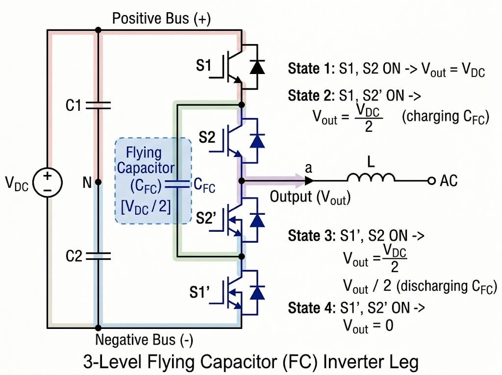
In a representative 3-level FC inverter leg operating from a total DC-link voltage of VDC, the circuit comprises two complementary pairs of switches: upper switches (S1, S2) and lower switches (S1′, S2′). A flying capacitor, CFC, is positioned between the midpoints of these switch pairs. Under nominal steady-state operation, the capacitor voltage is regulated to approximately half the DC-link voltage:
By controlling the gating signals of S1 and S2 (with S1′ and S2′ operated in complementary fashion, subject to suitable dead times), the phase-leg output voltage Vout (referenced to the negative DC rail) synthesizes three nominal voltage levels:
- State 1 (Level VDC): S1 = ON, S2 = ON. The phase output connects directly to the positive DC rail: Vout = VDC. The flying capacitor is bypassed and carries no load current.
- State 2 (Level VDC/2 – Charging Path): S1 = ON, S2 = OFF. Positive load current flows through S1 into CFC and returns through the lower complementary switch path, charging the flying capacitor: Vout = VDC – VC_FC ≈ VDC / 2.
- State 3 (Level VDC/2 – Discharging Path): S1 = OFF, S2 = ON. Positive load current discharges CFC through S2: Vout = VC_FC ≈ VDC / 2.
- State 4 (Level 0): S1 = OFF, S2 = OFF. The phase output connects directly to the negative DC rail: Vout = 0. The flying capacitor is bypassed.
Under balanced capacitor conditions, the nominal switch voltage stress across each semiconductor is reduced to:
Where N represents the number of voltage levels (N = 3 for a standard 3-level leg). It is important to emphasize that VDC / (N – 1) represents the idealized steady-state blocking voltage. During dynamic load steps, switching dead times, and when capacitor ripple is present, actual peak voltage stress includes transient margins. Nonetheless, this reduction allows engineers to evaluate lower-voltage rated MOSFETs or compact power modules such as the 2MBI100HA-120-50 half-bridge module, which exhibit favorable conduction resistance and reduced gate drive energy compared to higher-voltage discrete switches.
Voltage Balancing in FC Topologies: The Core Engineering Challenge
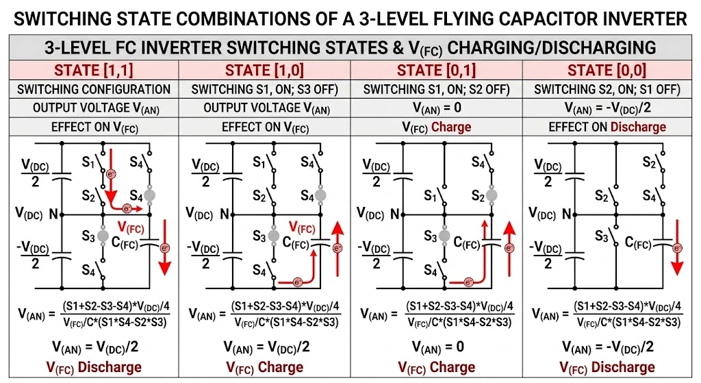
The primary structural merit of the FC converter—dividing blocking voltage across series-connected floating capacitors—is coupled with the challenge of capacitor voltage regulation. If the flying capacitor voltage VC_FC drifts from its target reference of VDC / 2, semiconductor voltage stresses become asymmetrical across the upper and lower complementary pairs.
For instance, if VC_FC drifts upward to 0.7 × VDC due to modulation asymmetries or transient current surges, switch S2 experiences an increased blocking voltage stress of 0.7 × VDC during its OFF interval. While the device may not immediately fail if designed with generous breakdown ratings, such voltage deviation compromises the intended safety margin, increases localized switching loss, and may exceed the device’s intended blocking-voltage margin or transient rating under peak line conditions. Furthermore, capacitor voltage imbalance introduces low-frequency harmonic distortion into the synthesized output waveform, complicating output filter attenuation and electromagnetic compliance.
Natural Voltage Balancing Mechanism via Phase-Shifted PWM (PS-PWM)
Flying Capacitor converters modulated with Phase-Shifted Pulse Width Modulation (PS-PWM) can exhibit an inherent self-balancing property under steady-state operating conditions. Comprehensive analytical treatments of this mechanism are documented in published literature, such as the classic IEEE study on Natural Balancing of Flying Capacitor Converters.
In an N-level FC leg, PS-PWM employs (N – 1) triangular carrier waveforms of identical switching frequency fsw and peak-to-peak amplitude, mutually displaced by a uniform phase angle:
For a 3-level leg, two carrier waveforms (Carrier 1 and Carrier 2) are displaced by 180°. Comparing these carriers against a common sinusoidal reference signal generates gating commands for S1 and S2.
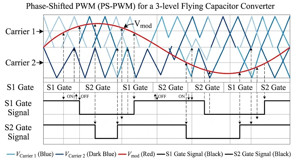
Under symmetrical steady-state conditions with linear passive loads, the time spent in redundant switching states (State 2 and State 3) balances out across fundamental periods. Over an integral AC line cycle, the net charge delivered to the flying capacitor converges toward zero:
If a minor perturbation shifts VC_FC slightly above VDC / 2, the impedance differences and phase timing during redundant intervals create a compensating current differential that drives the capacitor voltage back toward nominal.
Operating Limits of Natural Balancing:
It is vital to recognize that natural balancing is not an unconditional guarantee. Its restoring dynamics depend on:
- Modulation Index and Frequency Ratio: Natural balancing relies on sufficient redundant state transitions; at very low modulation depths or extreme frequency ratios, the restoring rate diminishes substantially.
- Load Impedance Characteristics: Highly non-linear loads, heavy DC-offset currents, or rapid step-load transients can overwhelm the natural passive balancing dynamics.
- Dynamic Settling Time: Passive natural balancing typically requires multiple fundamental AC cycles to correct substantial voltage offsets, which may prove too sluggish during inverter startup or grid fault ride-through events.
Active Voltage Balancing Strategies for Transient Robustness
To ensure deterministic operation under rapid load steps, startup charging, and grid-tied disturbances, modern digital controllers (such as 32-bit DSPs or FPGAs) incorporate closed-loop active balancing routines:
- Redundant State Selection (RSS): The controller samples VC_FC and phase current direction Iout. When synthesizing the intermediate voltage level, the algorithm selectively assigns either State 2 (charging) or State 3 (discharging) based on instantaneous voltage error and current polarity, actively forcing convergence within sub-cycle intervals.
- Duty Cycle Deviation Injection: A proportional-integral (PI) regulator computes a minor correction term Δd, which is added to individual switch carrier comparisons. This dynamically adjusts the relative duty ratio of redundant states to eliminate steady-state offsets without destabilizing the fundamental modulation.
| Control Strategy | Implementation Complexity | Transient Response Time | Hardware Sensor Requirement |
|---|---|---|---|
| Natural Balancing (PS-PWM) | Low (Open-loop) | Moderate to Slow (Multiple AC line cycles) | None |
| Redundant State Selection (RSS) | Medium | Fast (Sub-cycle response) | Flying Capacitor Voltage & Phase Current Sensors |
| Active Duty Cycle Injection | High | Fast (Continuous closed-loop) | Isolated Differential Voltage Sensors |
Wide Bandgap (WBG) vs. Multilevel Silicon Topologies: Engineering Trade-Offs
In high-efficiency power conversion—such as commercial string solar inverters, battery energy storage systems, and industrial motor drives—the choice between high-voltage Wide Bandgap (WBG) semiconductors and Multilevel Silicon configurations represents an application-dependent architecture trade-off rather than a universal rule.
1. Effective Frequency Multiplication and Passive Filtering
An advantageous property of the FC topology modulated with PS-PWM is interleaved carrier frequency multiplication. In an N-level FC converter where each semiconductor switches at a carrier frequency fsw, the ripple frequency observed by the output filter inductor is:
For a 5-level FC leg operating with individual silicon switches at fsw = 25 kHz, the output inductor experiences an effective ripple frequency of 100 kHz (4 × 25 kHz). Because the voltage step across the inductor is concurrently reduced to VDC / 4, the required filter inductance and core volume drop substantially, mitigating magnetic core losses.
By contrast, a conventional two-level inverter utilizing 1200 V SiC MOSFETs (such as those analyzed in our study on The 1200 V CoolSiC™ MOSFET Advantage in Three-Phase Power Conversion) must switch at high frequencies while withstanding full DC-bus voltage steps (dv/dt), placing greater demands on filter design and EMI shielding.
2. Architecture Comparison and Semiconductor Selection
The appropriate switch voltage rating depends directly on DC bus voltage, safety margins, switching transients, and chosen topology:
- Two-Level Implementations: On standard 400 V to 800 V DC buses, two-level topologies typically employ 650 V or 1200 V rated switches. For heavy industrial drives or grid-tied stages requiring robust margin, standard dual-pack modules such as the FS225R12KE3_S1 1200 V IGBT module illustrate traditional industrial two-level configurations. While two-level WBG designs simplify gate drive counts and PCB layout, SiC switches remain sensitive to parasitic loop inductance and can generate elevated high-frequency conducted EMI.
- Multilevel FC Implementations: By distributing a 400 V or 800 V bus across intermediate flying capacitors, individual switch blocking requirements drop significantly. In 400 V bus systems, a 5-level architecture may utilize lower-voltage Silicon MOSFETs, depending on the actual voltage-sharing and design margin. These lower-voltage devices benefit from mature manufacturing processes, offering low area-specific on-resistance. Detailed hardware evaluations, such as the Texas Instruments TIDUEI8 Reference Design, demonstrate that multilevel flying capacitor architectures can achieve high power density with compact filter inductors.
3. Conduction vs. Switching Loss Dynamics
The distribution between conduction and switching losses is not static; it depends on device figure-of-merit (FOM), switching frequency, RMS load current, and modulation depth:
- In multilevel FC converters, switching energy per transition is substantially reduced because each switch commutes across only a fraction of the bus voltage; switching energy generally decreases as the voltage swing per transition is reduced, although the actual loss depends on device characteristics and switching conditions.
- However, total conduction losses depend on the total on-state resistance of series-conducting switches. In topologies where multiple switches conduct simultaneously, conduction losses can become prominent under heavy load currents. Consequently, semiconductor selection must optimize on-resistance at elevated junction temperatures.
4. Thermal Distribution and Power Cycling Considerations
Thermal management represents another key differentiator. In a two-level design, power losses are concentrated in a few discrete switches, creating localized thermal hotspots and significant junction temperature swings (ΔTj) during cyclic load profiles.
In multilevel FC topologies, semiconductor losses are distributed across a greater number of surface-mount devices (such as PQFN, SuperSO8, or TO-LL packages) across the PCB. This expanded physical distribution allows internal copper planes to assist in thermal spreading. In systems operating within moderate ambient temperatures and well-ventilated enclosures, this distributed loss profile can reduce heatsink volume and simplify mechanical enclosures.
Engineering Component Selection Guidelines
Implementing a dependable Flying Capacitor converter requires careful selection of both passive components and active drive electronics.
1. Flying Capacitor Dimensioning and Dielectric Selection
Flying capacitors carry continuous high-frequency AC ripple currents. Selecting appropriate dielectric technologies is critical to prevent premature failure from Equivalent Series Resistance (ESR) self-heating.
Capacitance Sizing:
A simplified first-order estimate for minimum required flying capacitance CFC is expressed as:
Where Iout(peak) is peak phase current, fsw is switch carrier frequency, and ΔVC(max) is the maximum allowable voltage ripple (often specified as a small percentage of the nominal capacitor voltage, depending on the application).
Engineering Precaution: Designers must treat this equation as a preliminary first-order guideline. Actual required capacitance depends on the exact capacitor current waveform, modulation index, power factor, and redundant state sequence. Furthermore, when utilizing Class II Multi-Layer Ceramic Capacitors (MLCCs, such as X7R or X8R), engineers must account for the significant DC-bias capacitance derating, where effective capacitance can drop by 30% to 60% under nominal operating voltage. In higher-power systems, low-ESR high-frequency polypropylene film capacitors are frequently selected for their stable capacitance under DC bias and self-healing properties.
2. Power Semiconductor Device Criteria
When specifying switches for Flying Capacitor stages, engineers should evaluate:
- RDS(on) Temperature Coefficient: Prioritize devices with low on-resistance at expected junction operating temperatures (100°C–125°C) to keep total conduction dissipation bounded.
- Gate Charge (Qg and Qgd): Low gate charge reduces gate drive power requirements and facilitates clean switching transitions; for circuit techniques mitigating parasitic turn-on, refer to our technical discussion on Precision Gate Drive Design: Mastering Gate Charge and Miller Effect Mitigation.
- Package Parasitic Inductance: Select low-inductance surface-mount or planar packages to minimize high-frequency voltage overshoot across switching loops during rapid commutation.
3. Gate Driver Architecture and CMTI Considerations
Because the reference source/emitter nodes of upper switches in an FC topology float at high-frequency switching potentials, isolated gate drivers or dedicated bootstrap arrangements are necessary.
Common Mode Transient Immunity (CMTI) should be selected in direct alignment with anticipated circuit dv/dt and layout parasitics. While high-speed wide bandgap devices may demand CMTI ratings of 100 kV/μs or higher, multilevel silicon designs operating with lower individual voltage steps may operate reliably with moderate CMTI drivers, provided ground bounce and layout parasitics are tightly controlled. For detailed calculation methods, consult the Texas Instruments SLLA494 Application Report on High-Voltage CMTI.
Conclusion
The Flying Capacitor multilevel topology provides a viable engineering pathway for high-density, efficient power conversion. By taking advantage of Phase-Shifted PWM (PS-PWM), FC architectures benefit from natural steady-state voltage balancing and effective output ripple frequency multiplication.
Rather than being a universally superior approach to high-voltage Wide Bandgap (WBG) semiconductors, multilevel Silicon represents an architecture trade-off. While multilevel topologies increase gate drive circuit count and require flying capacitor voltage management, they enable the use of mature, low-voltage Silicon MOSFETs with low conduction resistance, reduce magnetic filter size, and distribute thermal losses across the circuit assembly. For design teams balancing efficiency targets, acoustic constraints, magnetic component volume, and semiconductor costs, the Flying Capacitor configuration remains an important topology in modern renewable energy and industrial power electronics.