
Mastering Power System Dynamics: Stray Inductance, Voltage Overshoot, and Snubber Design in High-Frequency Power Converters
In modern high-frequency power electronics, the quest for higher power density, faster switching speeds, and superior energy conversion efficiency has pushed semiconductor devices to their operational limits. Whether designing advanced electric vehicle (EV) onboard chargers, industrial motor drives, or high-efficiency induction heating systems, power electronic engineers frequently encounter a persistent adversary: parasitic inductance. When fast-switching power devices such as Insulated Gate Bipolar Transistors (IGBTs) or Silicon Carbide (SiC) MOSFETs turn off abruptly, trapped energy within circuit stray inductances generates severe voltage overshoots and high dv/dt transients. These transient phenomena threaten device reliability and can easily push operating loci outside the safe operating area (SOA). This technical article explores the root causes of stray inductance, analyzes voltage overshoot mechanisms, and details robust mitigation strategies including decoupling capacitors, RCD clamp circuits, and advanced snubber design.
1. The Physics of Stray Inductance and the DC Loop
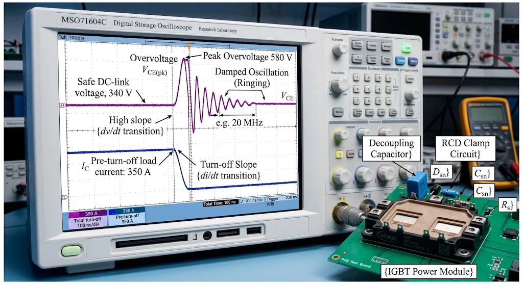
When a power semiconductor device transitions from a conducting state to a blocking state, the abrupt interruption of load current gives rise to transient overvoltages. The magnitude of this transient voltage is directly proportional to the total circuit stray inductance (often referred to as the DC loop inductance, LS) and the current fall rate (di/dt). This relationship is governed by the fundamental inductive voltage equation:
The situation becomes critical when utilizing fast-switching high-current modules. Higher-current power modules typically consist of multiple individual IGBT or MOSFET chips connected in parallel. Each individual chip switches its share of the load current at a di/dt dictated by the gate drive circuit and internal device characteristics. The aggregate current and di/dt experienced by the external power circuit represent the sum of currents through each parallel chip, frequently producing effective rates of change reaching several thousand amperes per microsecond (A/µs).
In standard through-hole semiconductor packages such as TO-220 or TO-247, physical lead pads introduce parasitic inductances. Specifically, the emitter lead inductance participates in both the high-power switching loop and the low-power control gate loop, creating common-source impedance coupling. Similarly, the power loop incorporates stray inductances originating from collector leads and printed circuit board (PCB) copper traces connecting switching devices to the DC-link capacitor bank. For demanding power switching stages requiring low internal parasitic inductance and balanced current sharing, standard industrial modules such as the Semikron SKM150GB12T4G dual IGBT module provide optimized internal lead geometries to mitigate package-level voltage stress.
2. Decoupling Capacitors and Low-Inductance Layout Strategies
Mitigating voltage transients at the source requires systematic minimization of the parasitic DC loop inductance. Preventive measures begin at the physical layout and component selection stages. Effective techniques include utilizing laminated copper busbars to cancel magnetic fluxes, minimizing physical loop surface areas, and choosing DC-link source capacitance with inherently low self-inductance.
For low and medium current applications, decoupling capacitors connected directly across the power module’s bus terminals provide an exceptionally effective remedy. Modern high-frequency polypropylene film capacitors are engineered with low-profile geometries designed to match standard IGBT and MOSFET terminal spacings for direct mounting. Because these capacitors eliminate conventional wire leads, their internal equivalent series inductance (ESL) is drastically lower than traditional leaded capacitors, allowing them to supply localized transient current spikes and clamp high-frequency ringing effectively.
3. RCD Clamp Circuits, Snubber Networks, and Energy Transfer
Even with optimized physical layouts, parasitic inductances cannot be entirely eliminated. Snubber networks and active clamping circuits are therefore essential to absorb trapped inductive energy and protect power switches. As detailed in the Texas Instruments Snubber Circuits Design Guide (SLUP100), proper snubber selection directly dampens oscillatory ringing and diverts peak turn-off energy away from semiconductor junctions.
In single-ended quasi-resonant (QR) converter topologies commonly deployed in induction cooking and high-frequency power supplies, the peak collector-emitter voltage (VCE) of the IGBT is not fixed; rather, it varies dynamically with the resonant load and output power. During Phase I and Phase IV operating cycles, the circuit behaves characteristically as an RL series circuit, where inductor current can be modeled by transient exponential growth:
Where Imax = VBUS / R, τ = L / R, and I0 represents the diode turn-on current. If insufficient energy is stored in the resonant inductor during IGBT turn-off, or if equivalent load resistance is high, the device voltage may fail to reach zero, resulting in hard-switching events during subsequent turn-on cycles. Hard-switching significantly increases total power dissipation, which can be estimated by the residual energy stored in the snubber capacitance multiplied by the switching frequency:
To curb turn-on voltage spikes and protect against grid surges or mains interruptions, engineers deploy specialized protection networks. Common solutions include:
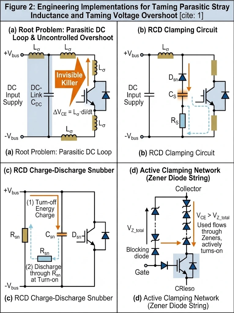
- RCD Charge-Discharge Snubbers: Comprising resistors, capacitors, and diodes that channel and dissipate energy released during device turn-off, effectively reducing VCE overshoots by over 150 V.
- Active Clamping Networks: Utilizing a series string of Zener diodes connected between the collector and gate terminals to actively turn on the IGBT when collector voltage exceeds safe thresholds, safely clamping transient voltage spikes.
- Metal Oxide Varistors (MOVs): Providing coarse voltage surge suppression against unpredictable grid fluctuations, though auxiliary snubber circuits remain necessary for high-speed switching transient absorption.
4. Dynamic Voltage Stress and Safe Operating Area (SOA) Limits
The Safe Operating Area (SOA) defines the capability of a power transistor to withstand simultaneous high levels of voltage and current without sustaining physical damage. In practical power conversion systems, semiconductor devices encounter severe combined stress during three primary operating conditions:
- Short-Circuit Events: Where device current is limited solely by gate voltage and transconductance, reaching magnitudes exceeding 10 times the continuous rating. Modern short-circuit-rated IGBTs achieve ruggedness by restricting hole current density and transconductance, though this trade-off typically results in a slightly higher on-state saturation voltage.
- Turn-Off Transients: Where inductive energy discharge forces the operating point toward the Reverse Bias Safe Operating Area (RBSOA) boundary.
- High dv/dt Switching: Rapid voltage transitions that test the dynamic dielectric and thermal limits of semiconductor chips.
Proper integration of decoupling and snubber networks ensures that dynamic operating trajectories remain well within rated SOA boundaries, preventing destructive second breakdown phenomena. Engineers must cross-examine manufacturer SOA curves under maximum junction temperature limits; refer to ROHM Technical Guidance on Transistor Safe Operating Area (SOA) Limits for in-depth boundary validation protocols.
5. Gate-Drain Coupling, Miller Capacitance, and Parasitic Turn-On
Beyond power loop overshoots, high dv/dt transients pose a secondary threat in bridge converter configurations: parasitic turn-on via internal device capacitances. This phenomenon is closely coupled with the Miller Effect; for practical gate-drive tuning and clamp circuitry, review our comprehensive engineering guide on Understanding Miller Effect and Parasitic Turn-On: Gate Drive Matching and Mitigation. Power transistors possess inherent terminal capacitances, including input capacitance (Cies = Cge + Cgc), output capacitance (Coes = Cce + Cgc), and reverse transfer or Miller capacitance (Cres = Cgc).
When one leg of a half-bridge circuit turns on rapidly, a steep collector-emitter voltage rise (high dv/dt) is imposed across the complementary off-state device. This rapid voltage rise injects a displacement current through the Miller capacitance (Cgc) directly into the gate terminal:
If the resulting voltage drop across the gate drive impedance exceeds the device threshold voltage (Vgs(th)), it can induce a spurious, unintended partial turn-on of the device, leading to destructive shoot-through currents and catastrophic bridge arm short circuits. To combat this, modern designs utilize low-impedance gate driver ICs, negative turn-off bias voltages, and advanced wide-bandgap devices such as Infineon CoolSiC MOSFETs featuring inherent immunity against parasitic capacitive turn-on and optimized unipolar gate drive compatibility.
| Parameter / Phenomenon | Primary Root Cause | Primary Consequence | Engineering Mitigation Strategy |
|---|---|---|---|
| Voltage Overshoot | Stray inductance (LS) · di/dt | Exceeds VCE breakdown rating | Decoupling capacitors, RCD snubbers |
| Parasitic Turn-On | Miller capacitance (Cgc) · dv/dt | Shoot-through currents, thermal runaway | Negative gate bias, low-impedance drivers |
| Switching Losses | Hard-switching and residual energy | Elevated junction temperature, reduced efficiency | Quasi-resonant soft-switching, optimized gate voltage |
6. Practical Engineering Selection Guidelines and System Reliability
Designing reliable power conversion hardware requires a holistic approach that harmonizes circuit layout, active device selection, and protective network design. When selecting power switches for high-performance topologies like LLC resonant converters or multi-level inverters, engineers must evaluate dynamic figures of merit such as output charge (Qoss), gate charge (Qg), and reverse recovery charge (Qrr) alongside static on-state resistance (RDS(on)).
Advanced semiconductor families and rugged industrial modules—such as the low-inductance Infineon FF200R12MT4 EconoDUAL™ 3 IGBT module and CoolMOS CFD7 devices with fast body diodes—provide exceptional resilience during critical operational phases including startup, burst mode, and output short-circuits. By pairing these advanced components with meticulously calculated RCD snubbers, low-inductance DC bus structures, and optimized gate drive layouts, power electronics engineers can successfully tame parasitic inductance, eliminate destructive voltage overshoots, and ensure long-term system reliability in demanding industrial and automotive environments.