Content last revised on September 12, 2026
SKM150GB12T4G Electrical Boundary Verification and Busbar Layout
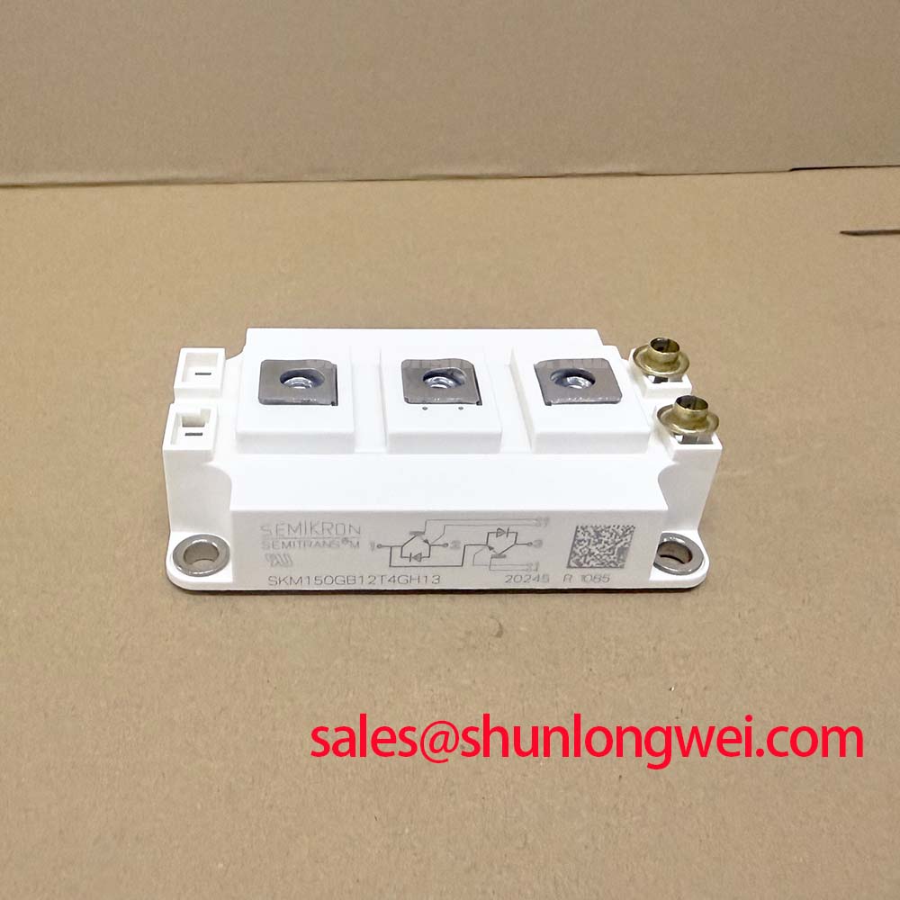
Begin a replacement inspection by recording the nameplate rating, checking the module body for visible mechanical damage, and confirming that the planned operating envelope remains within the documented limits of the Semikron SKM150GB12T4G. The available manufacturer-linked product data identifies this device as a 1200 V, 150 A IGBT module in a Semitrans housing. These are official product specifications; switching frequency, pulse current, short-circuit withstand, thermal resistance, gate voltage, and switching energy must be verified against the applicable Semikron documentation before a design review.
For a commercial string inverter or micro-grid energy storage converter, the module should be evaluated as part of the complete switching cell rather than as an isolated replacement. The DC-link voltage, modulation strategy, current waveform, cooling assembly, gate-driver configuration, protection response, and busbar geometry all influence the electrical stress applied to the device. Designers should verify the actual peak collector-emitter voltage during double-pulse and loaded switching tests, especially when the original busbar, snubber network, or gate driver has been modified.
Busbar symmetry is a practical first inspection point. Keep the commutation path compact, use a controlled forward and return-current path, and avoid routing the gate-drive return through a high-current emitter path. Stray inductance in the power loop can increase turn-off overshoot when current changes rapidly. The correct engineering approach is to minimize the parasitic loop area, then verify the resulting voltage margin with a suitably rated differential probe and an oscilloscope. A numerical inductance limit should come from the system switching target and measured transient behavior, not from a generic product-page assumption.
When several modules are used in a converter, current sharing requires attention to both static and dynamic behavior. The positive temperature coefficient commonly associated with IGBT conduction can support parallel operation, but it does not remove the need for matched mechanical mounting, symmetrical busbar impedance, consistent gate-loop geometry, and individually verified switching waveforms. Designers should compare collector current, gate-emitter voltage, turn-on delay, turn-off behavior, and temperature rise across each position under the intended operating conditions.
A semiconductor fuse may be part of the equipment protection architecture, but its coordination cannot be inferred from the module current rating alone. The fuse’s let-through energy, prospective fault current, DC-link characteristics, interruption capability, and the module’s documented short-circuit behavior must be considered together. Any I²t coordination claim requires the relevant fuse and module data sheets plus test validation under the intended fault circuit.
SKM150GB12T4G Short-Circuit Protection and Soft Turn-Off Coordination
Short-circuit protection for the SKM150GB12T4G should be designed around the equipment’s measured fault-current rise and the gate driver’s actual response delay. Desaturation detection, current sensing, or another documented protection method may be used, but the selected method must distinguish a genuine overcurrent event from switching noise and normal saturation behavior. The module’s short-circuit safe operating area and allowable protection timing must be taken from the applicable official technical documentation.
A fast protection response is useful only when the detection circuit, isolation barrier, driver output stage, and gate-loop layout work as one system. The sensing path should be physically separated from high-current commutation conductors, with a clear reference strategy and adequate noise immunity. During commissioning, inject controlled fault-like test conditions at reduced energy where possible, then capture the gate-emitter waveform, collector-emitter voltage, current waveform, and driver fault signal on the same time base.
Two-stage soft turn-off is an engineering recommendation that can reduce the voltage excursion caused by abruptly interrupting a high fault current. The first stage limits the rate of gate discharge, while a later stage completes turn-off after the current has fallen to a safer level. The correct delay and gate-current profile depend on the driver, DC-link voltage, loop inductance, load, and module operating point. They should be tuned from measured waveforms and checked against the manufacturer’s short-circuit and switching limits.
Clearance and creepage around the DC-link and phase terminals should follow the applicable equipment insulation standard, pollution level, working voltage, and enclosure conditions. A module’s voltage rating does not independently establish the insulation design of the complete inverter. Designers should also inspect the physical condition of busbar supports, terminal fasteners, insulating films, and capacitor connections after a protection event because an apparently intact module can be connected to a damaged commutation network.
For a neutral evaluation of related topology components, engineers may review the SKM75GB07E3 product information as a separate device reference. It should not be treated as an automatic substitute for the SKM150GB12T4G: voltage, current, topology, package geometry, gate-drive requirements, thermal path, and protection behavior must all be checked against the original equipment documentation.
Gate-Loop Waveform Tuning, Miller Coupling, and Dead-Time Verification
At the bench, first capture the gate-emitter voltage at the module terminals rather than at the driver board. This distinction matters because the gate-loop conductors can develop a different waveform from the driver output when common-emitter inductance and switching current interact. Ringing, an unexpected plateau, or a gate excursion during the opposite switch’s transition may indicate excessive loop impedance, measurement error, Miller coupling, or insufficient control of the complementary channel.
The collector-emitter transition can couple through the device’s effective reverse-transfer capacitance, often discussed in switching analysis as the Cres contribution. A high dv/dt event can inject current into the inactive gate loop. Active Miller clamp circuitry, a low-impedance gate return, careful source and power-return separation, and a properly referenced isolated driver can help reduce unintended turn-on. These are design considerations, not confirmed internal features or guaranteed operating functions of this specific module.
Gate resistance should be selected from the required switching loss, overshoot, EMI behavior, driver capability, and measured gate-current waveform. A common starting value from another design cannot be presented as a fixed SKM150GB12T4G requirement. Designers should tune turn-on and turn-off resistance independently where the driver permits it, then verify the resulting collector-emitter voltage, current overlap, junction-temperature estimate, and fault response.
Dead time must prevent simultaneous conduction of complementary devices while avoiding unnecessary diode conduction and recovery stress. The appropriate buffer is determined by driver propagation mismatch, temperature, load current, device switching behavior, and measurement tolerance. Verify it across the full operating range instead of validating a single room-temperature waveform. The interlock signal, isolated power supply behavior, fault reset logic, and gate-enable state should also be checked during power-up, brownout, and fault recovery.
The SKM150GB12T4G gate-drive supply voltage and any negative turn-off bias must be confirmed from the original Semikron documentation and the existing converter design. Do not assume a generic IGBT gate voltage or negative-bias value is suitable. Before connecting a replacement module, compare the driver’s peak source and sink current, UVLO behavior, isolation rating, clamp operation, and connector pin assignment with the equipment schematic.
Where the converter includes a separate rectifier or front-end stage, the SKM100GB063D reference may help engineers map the broader power topology. It remains a separate component record; compatibility must be established from circuit function and verified ratings rather than product-family appearance.
Commissioning Diagnostics for Isolation, Common-Mode Transients, and Thermal Contact
Commissioning should begin with the DC bus discharged and the gate-driver supply isolated from the power stage. Check terminal identification against the original equipment drawing, inspect the gate-emitter path for unintended continuity, and confirm that the driver does not enable the switch while the protection circuit is reporting a fault. After low-energy functional checks, increase test conditions gradually while monitoring gate-emitter voltage, collector-emitter voltage, phase current, heatsink temperature, and fault timing.
Common-mode transients can disturb an isolated gate driver when the power loop and control loop share excessive electric-field coupling or when the isolation layout is poorly referenced. The necessary common-mode transient immunity, reinforced isolation performance, clearance, creepage, and insulation system are properties of the driver and converter assembly, not automatically of the IGBT module. Designers should verify the driver data sheet, PCB insulation design, enclosure contamination conditions, and the complete system test results.
If a gate signal appears during the opposite device’s transition, investigate the measurement reference, driver supply decoupling, interlock timing, gate-return impedance, clamp function, and power-loop coupling together. A single waveform symptom does not establish one definitive failure cause. Compare the suspect channel with a known-good channel under matched operating conditions, and repeat the test with controlled changes to the driver enable state and switching speed.
The manufacturer’s SEMITRANS Industry Standard IGBTs information provides useful package and product-family context, while the Semikron-Danfoss Power Electronics and Modules hub should be consulted for current manufacturer documentation. These references do not replace the exact technical data required for the SKM150GB12T4G installation.
Thermal commissioning requires an uninterrupted mechanical path from the module baseplate to the heatsink. Clean both contact surfaces using an approved process, apply the selected thermal interface material consistently, and inspect for trapped contamination or uneven spreading. The interface thickness, allowable surface flatness, baseplate behavior, and mounting sequence should follow the module documentation and the heatsink supplier’s requirements. The objective is uniform contact pressure without distorting the package.
Install fasteners in a gradual diagonal sequence using a calibrated torque tool and the documented hardware specification. 🔧 Pro Tip: Disconnect all power sources and verify the DC link is discharged before touching gate, power, or auxiliary connectors. After assembly, check that the module sits flat, the busbars are not forcing terminal misalignment, and the thermal interface has not been displaced by mechanical stress.
Record thermal resistance assumptions separately from measured temperatures. A rising case temperature may involve insufficient airflow, poor interface contact, overload, switching loss, sensor placement, or an abnormal current-sharing condition. Verify each possibility with measured electrical and mechanical evidence before replacing additional parts. For structured guidance on gate-drive routing, thermal integration, and power-stage troubleshooting, consult IGBT Design & Integration.