

Content last revised on November 18, 2026
SEMIX223GB12E4P Circuit Protection & Reliability: Calibrating Turn-Off Overshoot and Clamping
Isolate the power stage, verify that the DC link has discharged, and compare the cold-state readings across corresponding power terminals before reconnecting the gate driver. For the SEMIX223GB12E4P, record the disconnected terminal measurements alongside the equipment schematic; a low-resistance path can involve the module, an external snubber, or another connected branch, so an in-circuit reading alone cannot establish the failed component.
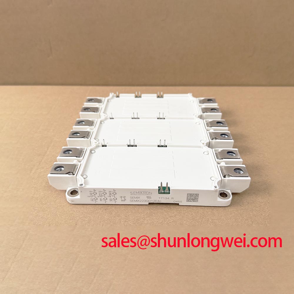
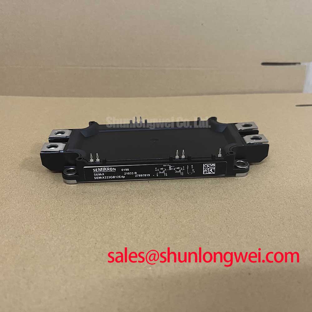
The product identification and primary specifications are: Manufacturer: Semikron; Part Number: SEMIX223GB12E4P; Collector-Emitter Voltage (Vces): 1200.0 V; Continuous Collector Current (Ic): 225.0 A; Package: SEMiX Module; Configuration / Topology: IGBT Power Stage. These are the product’s specified ratings, not a complete operating envelope. Consult the datasheet for the circuit diagram, rating conditions, terminal assignments, switching characteristics, and mounting requirements when checking a replacement against the original assembly.
Capture collector-emitter voltage during turn-off with a suitably rated differential measurement arrangement, keeping the probe connection loop short enough to avoid confusing measurement ringing with actual device stress. As a Design Consideration, compare the waveform at the module terminals with the DC-link waveform under the same switching event. Their difference helps distinguish local commutation-loop overshoot from a rising supply bus.
The relevant Engineering Calculation is that peak collector-emitter voltage is approximately the DC-link voltage plus stray loop inductance multiplied by the magnitude of current fall rate. This relationship explains why faster turn-off can increase overshoot even when the supply voltage is unchanged. It does not establish a universal busbar-inductance target or clamp setting; those depend on the actual current path, switching conditions, and verified device limits.
Inspect the return path between the local DC-link capacitor and the switching stage. Broad, closely coupled outgoing and return conductors can reduce loop inductance, but insulation spacing, terminal geometry, and mechanical support must remain appropriate to the assembly. Compare the repaired layout with the original arrangement, especially where replacement cables, displaced capacitors, or altered terminal hardware have enlarged the commutation loop.
For snubber evaluation, check pulse-current capability, repetitive dissipation, connection inductance, and the measured ringing response rather than selecting capacitance from the module current rating. Active clamping also needs coordination with the gate driver: clamp activation changes switching energy and must not be treated as permission for repetitive operation beyond the device envelope. The The 7th Generation IGBT Technical Reference provides broader switching-technology context; it does not establish the semiconductor generation or protection settings of this particular part.
SEMIX223GB12E4P Operational Boundaries: Evaluating Thermal Interface Thickness Uniformity
Inspect the heatsink contact surface for residual compound, raised burrs, contamination, and uneven contact marks before installing the SEMiX Module. As a Design Consideration, the thermal interface should fill surface irregularities without becoming an unnecessarily thick thermal barrier. Determine the application method and permitted interface thickness from the module mounting instructions and the selected thermal material’s requirements, rather than imposing a generic coating thickness.
Check surface flatness against the assembly requirements before attempting to compensate for a contact gap with additional compound. A visible contact-pattern difference can help locate uneven seating, but it does not by itself quantify thermal resistance. Follow the specified tightening sequence and torque with the appropriate hardware, avoiding uneven loading as the module seats against the heatsink.
Field Alert: Do not compensate for poor heatsink contact by increasing screw torque beyond the applicable module mounting specification.
After assembly, evaluate the cooling path under controlled loading, including coolant or airflow condition, heatsink temperature, and the relationship between load changes and thermal response. The 225.0 A current specification should be interpreted with its thermal test conditions; it is not an unconditional cabinet output-current setting.
Fuse coordination belongs in the same operating-boundary review. Compare the selected semiconductor fuse’s time-current behavior and total clearing I²t with the protection requirements and documented withstand characteristics of the complete power circuit. A fuse can limit fault energy without necessarily protecting an IGBT against every short-circuit event. Fast electronic fault detection and the upstream protective device therefore perform different roles and need coordinated validation.
Transient Dynamics & Electrical Design: Long Motor Lead Reflected-Wave Voltage on SEMIX223GB12E4P
Measure switching waveforms at both the inverter output and the motor terminals when investigating cable-dependent overvoltage. As a Design Consideration, impedance discontinuities between the cable and motor can reflect fast voltage edges, producing motor-terminal stress that differs from the voltage measured at the module. Keep these observations separate from collector-emitter turn-off overshoot; the locations and mitigation measures are not interchangeable.
Record cable routing, cable construction, motor connection, grounding arrangement, and any existing output reactor or filter before changing the installation. Evaluate a proposed dv/dt filter or choke against the drive manufacturer’s permitted output network, switching behavior, load current, and thermal requirements. Filter suitability depends on the connected system, not simply on matching the module’s voltage class.
When evaluating compatibility with a heavy-duty variable-frequency AC motor drive, compare the exact circuit diagram, terminal positions, driver interface, cooling arrangement, and control requirements. Background on Permanent Magnet Synchronous Motor (PMSM) Drives and Space Vector Modulation (SVM) in Three-Phase Motor Inverters helps explain system operation, but neither establishes compatibility with this module.
If procurement is also comparing the SEMIX453GB12E41P, treat it as a separate engineering comparison rather than an approved drop-in replacement. Match the electrical circuit, mechanical interfaces, switching behavior, and protection requirements before authorizing a substitution.
Transient Dynamics & Electrical Design: High-Speed Fault Management and VCE Desaturation on SEMIX223GB12E4P
Check the desaturation sensing path, blanking behavior, and driver fault response before restoring full-power operation after a switching-stage failure. As a Design Consideration, distinguish a short circuit already present at turn-on from a fault developing during conduction: the collector-voltage trajectory and detection sequence can differ. Set the protection timing against the documented short-circuit operating limits and actual driver delays, not a generic microsecond target.
Examine gate-emitter waveforms during complementary switching for unintended turn-on. Reverse-transfer capacitance couples collector-voltage movement into the gate circuit, while gate-loop impedance and driver sink capability determine the resulting disturbance. Dead time should prevent overlap under the relevant propagation delays and switching conditions; excessive dead time can also affect output behavior. Validate the timing at the device terminals rather than relying only on controller commands.
Where the driver supports staged or soft fault turn-off, evaluate its ability to reduce current without producing excessive collector-emitter overshoot. Slower shutdown can reduce inductive voltage stress while increasing fault energy, so the shutdown profile and clamp behavior require coordinated assessment. Finish the repair check by confirming fault latching, complementary-switch inhibition, and controlled restart behavior without repeatedly applying destructive faults to the power stage.