
In high-power switching applications such as industrial motor drives, solar inverters, and electric vehicle traction converters, power semiconductors operate under demanding dynamic conditions. While modern Insulated Gate Bipolar Transistors (IGBTs) and Silicon Carbide (SiC) MOSFETs continue to achieve faster switching speeds to minimize dynamic power losses, rapid transient voltage swings expose gate drive circuits to severe parasitic vulnerabilities. Chief among these operational risks is parasitic turn-on—often termed false turn-on or dV/dt-induced shoot-through—which occurs when high transient voltage gradients induce unwanted currents through inter-electrode capacitive paths. Understanding the underlying semiconductor physics and implementing rigorous gate drive impedance matching are fundamental prerequisites for engineering failure-resistant power conversion systems.
The Physics of Parasitic Turn-On in Power Switches
To grasp how a non-conducting semiconductor switch can prematurely enter a conducting state, power electronics designers must analyze the intrinsic parasitic capacitance network that defines the physical structure of MOSFETs and IGBTs. Every three-terminal power semiconductor exhibits three primary inter-electrode capacitances:
- Input Capacitance (Ciss): Defined as Cgs + Cgd (with Cds shorted), representing the total capacitance seen from the gate terminal.
- Output Capacitance (Coss): Defined as Cds + Cgd, dictating the energy stored across the switch during the OFF-state.
- Reverse Transfer Capacitance (Crss or Cgd): The critical Miller capacitance that couples the high-voltage collector/drain terminal directly to the sensitive low-voltage gate electrode.
Understanding these parasitic capacitance ratios is essential when evaluating advanced silicon and WBG devices; technical specifications can be cross-referenced with Infineon Gate Driver Solutions.
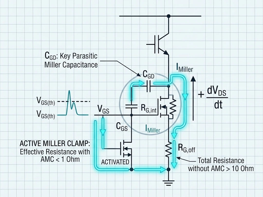
During normal operation in a half-bridge or phase-leg topology, one switch (the high-side switch) turns ON while the complementary complementary device (the low-side switch) remains commanded OFF with zero or negative gate voltage. As the high-side switch turns ON, the voltage across the low-side switch rapidly rises from nearly zero to the high-voltage DC bus level. This abrupt change in collector-to-emitter or drain-to-source voltage generates a steep transient voltage gradient across the OFF-state device, mathematically expressed as dVCE/dt or dVDS/dt.
Because the Miller capacitance Cgd directly bridges the high-voltage collector and gate node, this dynamic voltage variation drives a parasitic displacement current (IMiller) directly into the gate circuit. The magnitude of this current follows the fundamental electrostatic relationship:
IMiller = Cgd × (dVCE / dt)
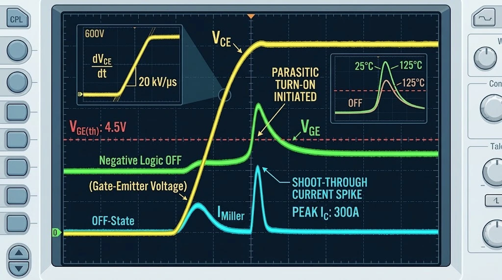
This displacement current must flow to electrical ground through the available path provided by the internal gate loop resistance, printed circuit board (PCB) traces, and the gate drive IC output stage. As IMiller flows through the total gate resistance, it creates an instantaneous voltage drop that elevates the internal gate voltage (VGE) above ground potential. If this induced transient voltage spike exceeds the device’s gate-emitter threshold voltage (VGE(th)), the OFF-state device initiates conduction. This creates a temporary short-circuit condition across the DC bus—commonly referred to as bridge shoot-through—leading to massive peak current surges, extreme thermal stress, and potential catastrophic device failure.
Key Circuit Parameters Influencing dV/dt Immunity
The susceptibility of a power stage to parasitic turn-on depends on a combination of semiconductor device characteristics and external gate loop design parameters. Analyzing these factors enables engineers to establish adequate design margins during component selection.
| Parameter | Physical Role in Parasitic Turn-On | Design Objective for High Immunity |
|---|---|---|
| Miller Capacitance (Cgd) | Determines the amount of displacement charge coupled to the gate per unit time. | Select switches with minimized Cgd or optimized Cgs/Cgd ratio. |
| Threshold Voltage (VGE(th)) | Defines the minimum gate voltage required to form a conductive channel. | Choose devices with higher VGE(th) or account for thermal degradation. |
| Internal Gate Resistance (RG,int) | Internal semiconductor structure resistance that cannot be reduced externally. | Minimize RG,int by selecting advanced chip geometries like trench structures. |
| External Gate Resistance (RG,ext) | External resistor used to tune switching speed and damping. | Optimize separate turn-ON and turn-OFF paths to decouple switching speed from immunity. |
| Gate Loop Parasitic Inductance (LG) | PCB trace inductance that causes gate voltage ringing and delays clamping response. | Minimize loop area using tight kelvin connections and ground planes. |
A crucial dynamic parameter often overlooked is the temperature dependence of VGE(th). As power devices heat up under nominal operating conditions, their threshold voltage typically exhibits a negative temperature coefficient, decreasing by several millivolts per degree Celsius. Consequently, an IGBT or MOSFET that provides acceptable dV/dt immunity at room temperature (25°C) may experience parasitic turn-on at elevated junction temperatures (125°C to 175°C) due to a reduced noise margin. Engineers evaluating gate drive immunity must calculate voltage margins using the minimum VGE(th) at maximum rated junction temperature. To learn more about comprehensive gate drive layout practices and parametric evaluations, review our 5 practical tips for robust IGBT gate drive design.
Quantitative Analysis of Gate Voltage Rise
To quantify the transient voltage spike generated at the gate during high dVCE/dt transients, the gate circuit can be modeled as an RC network driven by a current source. The peak gate-emitter voltage rise (ΔVGE) can be expressed by the fundamental steady-state approximation:
ΔVGE = IMiller × RG,total = Cgd × (dVCE / dt) × (RG,int + RG,ext + Rdriver)
Where Rdriver represents the internal sink impedance of the gate driver output stage. To guarantee that parasitic turn-on does not occur, the maximum transient gate voltage must remain below the minimum threshold voltage:
ΔVGE < VGE(th, min)
Consider a practical engineering example involving an industrial inverter operating at a DC bus voltage of 800 V. Assume the high-side switch transitions rapidly, imposing a dVCE/dt of 20 kV/μs (20 V/ns) across the low-side switch. If the power switch has a reverse transfer capacitance Cgd of 100 pF and the total gate turn-OFF resistance (RG,int + RG,ext + Rdriver) is 15 Ω:
IMiller = 100 × 10-12 F × 20 × 109 V/s = 2.0 A
This simplified calculation provides a first-order estimate. In an actual power device, the the actual Miller-induced gate-voltage transient is also influenced by the nonlinear Cgd characteristic, gate-driver impedance, parasitic inductance, and operating conditions.
ΔVGE = 2.0 A × 15 Ω = 30 V
Because 30 V far exceeds the typical threshold voltage of IGBTs (typically 5.0 V to 6.5 V) or SiC MOSFETs (typically 2.0 V to 4.5 V), the device will experience severe parasitic turn-on and shoot-through. This calculation demonstrates why standard unipolar gate drivers with moderate gate resistance are insufficient for controlling high dV/dt transients. For deeper insight into device-level dynamic specifications, consult our engineering guide on decoding IGBT datasheets.
Detailed mathematical models and analytical calculations for dV/dt-induced displacement currents are widely documented in published research across IEEE Transactions on Power Electronics.
Mitigation Strategies and Drive Impedance Matching
Preventing dV/dt-induced shoot-through requires strategic modifications to either the gate drive hardware architecture, the gate loop impedance, or the bias voltage levels. The primary industry-proven techniques include driving impedance optimization, split-gate resistor arrangements, parallel clamping diodes, active Miller clamping, and negative gate bias topologies.
1. Drive Impedance Matching and Asymmetric Gate Resistors
A simple approach to reducing gate voltage bounce is lowering the external turn-OFF gate resistance (RG,off). By utilizing asymmetrical gate drive configurations—where separate resistors are used for turn-ON and turn-OFF via an anti-parallel diode—designers can independently optimize switching speeds and dV/dt immunity.
Reducing RG,off lowers the overall impedance of the path through which IMiller discharges, reducing the peak voltage rise at the gate terminal. However, this method is fundamentally limited by the semiconductor switch’s unalterable internal gate resistance (RG,int). If RG,int itself is relatively high, minimizing external resistance yields diminishing returns.
2. Parallel Schottky Diode Clamping
To bypass the external turn-OFF gate resistor entirely during high dV/dt transients, a low forward-voltage Schottky diode can be placed in parallel with RG,off, oriented with its cathode facing the gate driver output. When a positive dVCE/dt induces current into the gate, the Schottky diode becomes forward-biased, shunting the current around RG,off directly into the low-impedance sink transistor of the gate driver. This arrangement reduces the effective external resistance to the diode’s dynamic resistance plus the driver’s internal sink resistance, lowering the peak gate voltage spike.
3. Active Miller Clamp (AMC) Circuits
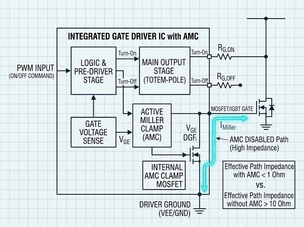
For applications operating with high dV/dt requirements, modern gate driver ICs integrate an Active Miller Clamp (AMC) feature. An AMC circuit continuously monitors the gate-emitter voltage during the OFF-state. When VGE drops below a predefined threshold (typically 2.0 V relative to ground or negative supply) during the turn-OFF transition, an auxiliary internal low-impedance switch (usually an internal N-channel MOSFET) connects the gate directly to the negative rail or driver ground.
By bypassing the main turn-OFF resistor, the Active Miller Clamp provides a path with impedance close to zero ohms directly at the driver pin. This clamps the gate potential tightly to the ground reference, effectively suppressing Miller displacement current before it can charge the gate-emitter capacitance above VGE(th).
For additional circuit design details and IC implementations, engineers can refer to the Texas Instruments Power Management Gate Driver Documentation.
Designing robust gate drive circuits with adequate dV/dt immunity requires selecting proven semiconductor devices. The following 1200V dual IGBT modules are widely specified in high-power industrial inverters and motor drives:
4. Negative Gate Bias Off-State Driving
Applying a negative gate bias voltage (e.g., -5 V, -8 V, or -15 V) during the OFF-state provides a dedicated safety voltage margin against parasitic turn-on. When a negative bias is applied, any Miller-induced voltage spike must first overcome this negative potential before reaching the positive threshold voltage VGE(th).
For example, if a system utilizes a -5 V negative bias and has a VGE(th) of +5 V, the effective noise margin increases from 5 V to 10 V. This allows the circuit to tolerate double the displacement current or dV/dt gradient before initiating conduction. Negative voltage driving is standard in high-power IGBT modules and high-speed SiC MOSFET converters where extreme dV/dt levels are routinely encountered. For a comprehensive review of semiconductor selection criteria across topologies, refer to our guide on power semiconductor selection frameworks.
To safely manage lower threshold voltages in high-speed SiC power stages, negative bias driver setups are thoroughly analyzed in STMicroelectronics Gate Driver Technical Resources.
Comparative Evaluation of Mitigation Techniques
Selecting the optimal mitigation strategy requires evaluating performance, component count, PCB area, and overall system cost. The following comparative analysis outlines the engineering tradeoffs associated with each technique:
| Mitigation Strategy | Effective Impedance Reduction | Added Component Complexity | dV/dt Immunity Level | Primary Application Fit |
|---|---|---|---|---|
| Asymmetric RG (Diode + Resistor) | Moderate (Limited by RG,ext) | Very Low (1 Diode, 1 Resistor) | Low to Moderate | Low-cost industrial drives, consumer power supplies |
| Parallel Schottky Clamp | High (Bypasses RG,ext) | Low (1 Schottky Diode) | Moderate | Medium-power inverters without negative rails |
| Active Miller Clamp (AMC) | Very High (Bypasses external path) | Low (Integrated into driver IC) | High | High-density industrial drives, Automotive EV inverters |
| Negative Off-State Bias (-VGS) | N/A (Increases voltage margin) | Moderate to High (Dual power rail needed) | Very High | High-voltage IGBT modules, high-speed SiC power stages |
Layout Best Practices to Prevent PCB-Level Parasitic Coupling
Even a well-designed gate drive schematic can fail if the physical PCB layout introduces significant parasitic inductance or capacitive cross-talk. To preserve dV/dt immunity in physical hardware, power engineers should adhere to several critical layout guidelines:
- Minimize Gate Loop Area: Trace loop area directly scales with parasitic inductance (LG). Route the gate drive signal and gate return (Kelvin emitter/source) directly on top of each other on adjacent PCB layers to maximize magnetic flux cancellation.
- Implement Dedicated Kelvin Emitter Connections: Always route the gate driver ground directly to the switch’s Kelvin emitter pin rather than the main power ground trace. This prevents high dI/dt main power loop currents from injecting transient voltages into the gate driver return path.
- Locate Driver IC and AMC Clamps Proximally: Minimize physical trace length between the gate driver output (or AMC pin) and the gate terminal of the power switch. Long traces add parasitic inductance that degrades the clamping response time during rapid transients.
- Avoid Capacitive Coupling Over Low-Side Gate Traces: Never route high-voltage switching nodes (such as the phase node or high-side drain) directly above or parallel to sensitive low-side gate traces. Ensure solid ground shielding layers separate high dV/dt power planes from low-voltage gate drive signals.
For additional details regarding gate drive interface circuits, high-speed layout strategies, and gate charge optimization methods, designers can consult external technical references such as Infineon Technologies Power Management Documentation.
Conclusion
Parasitic turn-on induced by the Miller effect remains a primary reliability challenge in high-speed, high-voltage power conversion systems. As modern semiconductor devices continue to push switching speeds higher to maximize efficiency, managing displacement current through Cgd becomes increasingly critical. By understanding the physical capacitive coupling mechanisms, calculating transient voltage rises quantitatively, and implementing targeted mitigation solutions—such as low-impedance Active Miller Clamps, asymmetric gate resistance, or negative supply bias—engineers can eliminate dV/dt-induced shoot-through risks. Combining these circuit-level design choices with tight, low-inductance PCB layout practices ensures stable, highly efficient, and long-term reliable operation across industrial and automotive power platforms.