
In high-power electronics, maintaining robust switching stability and preventing false turn-on events are primary concerns for design engineers. Power semiconductor switches such as Insulated Gate Bipolar Transistors (IGBTs) and Silicon Carbide (SiC) MOSFETs operate in noisy, high-power switching environments where high rate-of-change voltage transients (dv/dt) occur continuously. While modern silicon power MOSFETs and standard IGBT modules are theoretically designed to turn off cleanly at zero volts (VGS = 0V), practical circuit noise, parasitic inductances, and Miller capacitance spikes often threaten to pull the gate voltage above the device threshold.
To eliminate the risk of shoot-through currents and unwanted conduction in high-reliability power converters, implementing a negative gate bias during the off-state serves as an indispensable fail-safe mechanism. Over the years, gate drive design topology has evolved significantly. Circuit designers have transitioned from discrete, high-component-count charge pump circuits to clever passive biasing methods using standard driver ICs, and finally to modern dedicated integrated gate drivers. This technical guide explores the engineering principles, mathematical foundation, topology evolution, and design criteria for negative off-bias gate drive circuits.
1. Why Negative Gate Bias Matters: Parasitic Miller Capacitance and Noise Immunity
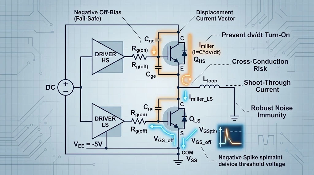
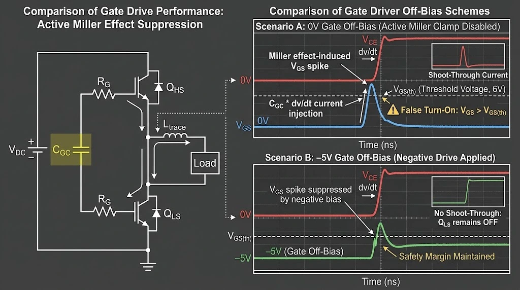
In bridge converter topologies—such as half-bridge, full-bridge, and three-phase motor drives—high-side and low-side power switches toggle alternately. When one switch turns on rapidly, it induces a very high voltage change over time (dv/dt) across the opposing off-state switch. This rapid transient causes a displacement current to flow through the parasitic gate-to-drain (or gate-to-collector) capacitance, commonly known as the Miller capacitance (Cgd or Cgc) (detailed in technical publications on 7th Generation IGBT Switching Dynamics).
The displacement current Imiller generated by this voltage transient can be expressed as:
Imiller = Cgd * (dv / dt)
This displacement current flows through the off-state driver output impedance and the series gate resistor (Rg), returning to ground. As a result, a transient voltage pulse develops across the gate-to-source terminals of the off-state transistor:
VGS(transient) = Imiller * Rg = Cgd * (dv / dt) * Rg
If VGS(transient) exceeds the device threshold voltage VGS(th), the off-state switch partially turns on while the opposite switch is conducting. This creates a direct short circuit across the high-voltage DC bus—a catastrophic phenomenon known as cross-conduction or shoot-through. Applying a negative off-bias voltage (such as -3V, -5V, or -10V) pulls the baseline gate voltage well below zero. Consequently, even if a Miller voltage spike occurs, the peak transient voltage remains safely under VGS(th), providing a solid safety margin against noisy environment triggers.
2. Early Solutions: Discrete Charge Pump Gate Drives
Before standard integrated high-voltage gate drivers supported negative power rails natively, engineers relied on discrete charge pump circuits to generate negative bias. These circuits were built using discrete BJTs, small-signal MOSFETs, steering diodes, and flying capacitors to shift the control signal level and supply negative potential.
Operating Principle of the Charge Pump Circuit
A classic discrete negative charge pump operates by AC-coupling the incoming pulse-width modulation (PWM) drive signal through coupling capacitors (C3, C4) and clamping the voltage levels using signal diodes (D3, D4). During the low phase of the incoming signal, energy is stored in the flying capacitor; during the high phase, the charge is transferred to generate a negative DC potential relative to the device emitter/source reference node.
| Component Group | Primary Function in Discrete Pump | Design Challenges |
|---|---|---|
| Coupling Capacitors (C3, C4) | Transfer AC pulse energy across DC isolation boundary | Voltage rating stress, duty-cycle dependency |
| Steering Diodes (D3, D4) | Rectify incoming signal to establish negative DC bias | Diode forward voltage drop (Vf) reduces net negative voltage |
| Level-Shifter Stage (Q1, Q2, D2) | Translate control signals to negative rail potential | High discrete component count, larger PCB footprint |
| Buffer Output Transistors (Q3, Q4) | Deliver peak current spikes during gate charge/discharge | Thermal dissipation, risk of shoot-through in discrete buffer |
Engineering Limitations of Discrete Charge Pumps
While discrete charge pumps successfully generate negative gate voltage without requiring an extra secondary winding on the auxiliary power supply, they present significant drawbacks:
- Duty Cycle Sensitivity: The magnitude of the generated negative bias voltage strongly depends on the switching frequency and duty cycle. At extreme duty cycles (e.g., less than 5% or greater than 95%), the charge pump may fail to refresh adequate negative voltage.
- High Component Count: Requiring over ten discrete resistors, capacitors, diodes, and complementary transistors drastically reduces system reliability and increases assembly costs.
- Poor Dynamic Regulation: Variations in load current and signal source output impedance lead to fluctuating negative bias levels.
3. Passive Generation: High-Side Bias via Standard Control ICs and Zener Diodes
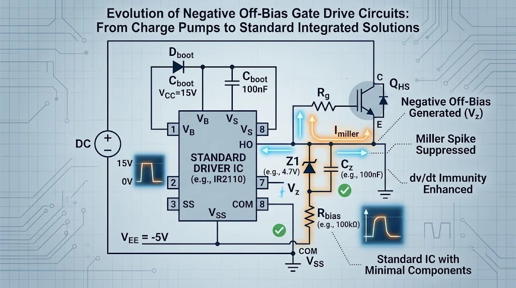
To overcome the complexity of discrete charge pumps, power electronics engineers developed simplified biasing topologies utilizing standard high-voltage bootstrap driver ICs (such as the classic IR2110 series) combined with basic passive networks. This technique generates a high-side negative turn-off voltage economically without requiring complex multi-output transformer power supplies.
For more detailed technical specifications on power control components, you can explore the SLW-ELE Official Product Catalog.
Circuit Architecture and Operation
In this architecture, an external negative voltage supply (e.g., -5V) is connected to the ground reference pin of the low-side system, while a Zener diode and capacitor network is integrated into the floating bootstrap loop.
- Floating Bias Setting: A Zener diode (D1, e.g., 4.7V) and a parallel decoupling capacitor (100 nF) are placed between the driver high-side return pin (VS) and the power transistor reference emitter/source node.
- Negative Voltage Shift: A pull-down resistor (e.g., 100 kΩ) connected to the negative power rail (-5V) sets the steady-state bias level.
- Charge Balancing: When the driver IC pulls the high-side output (HO) low, the gate is pulled to the VS pin potential, which sits below the emitter potential by the Zener voltage Vz. Thus, the gate experiences a constant negative turn-off bias.
This approach allows engineers to drive medium-power IGBTs and standard power transistors with minimal extra components, retaining the low cost of off-the-shelf control ICs while adding robust noise immunity.
📌 Benchmarking Real-World IGBT Modules Requiring Negative Gate Bias
In industrial motor inverters and heavy power conversion systems, specific standard dual-pack and PIM IGBT modules illustrate these design constraints in practice:
- Medium-Power Standard Dual Packs: The 2MBI150F-120 (1200V / 150A) frequently employs a -5V to -10V off-state bias in three-phase inverter bridges to suppress high-side switching dV/dt displacement spikes.
- High-Power Industrial Inverters: The CM400HA-24H (1200V / 400A single switch) features higher gate charge characteristics, where negative bias provides critical noise margin against heavy busbar parasitic ringing.
- Integrated Power Modules (PIM): In compact space-constrained drives, seven-pack modules like the 7MBR50SA120-50 (1200V / 50A) and SKM75GB12F4 (1200V / 75A) benefit from low-component Zener-biased high-side drive topologies to maintain high power density without discrete charge pumps.
4. Modern Standard Integrated Solutions
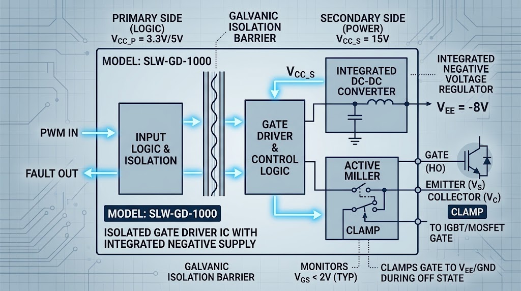
As switching frequencies increased with the adoption of wide-bandgap (WBG) materials like Silicon Carbide (SiC) and Gallium Nitride (GaN), traditional passive networks became insufficient. Modern power converter architectures require tightly regulated, high-speed negative gate bias to handle extreme dv/dt rates without excessive switching losses. Today, integrated gate driver ICs feature built-in negative rail generators and active Miller clamps.
Key Features of Modern Integrated Gate Driver ICs
- Integrated Negative DC-DC Controllers: Modern driver ICs incorporate small integrated charge pump or buck-boost controllers that generate precise negative rails (e.g., -3V, -4V, or -8V) dynamically across all duty cycles.
- Active Miller Clamping: Instead of relying solely on negative voltage, integrated drivers include an dedicated active Miller clamp pin (CLAMP). During turn-off, when the gate voltage falls below a specific threshold (e.g., +2V relative to ground), an internal low-impedance switch shorts the gate directly to the negative supply rail or ground, bypassing the external series gate resistor Rg.
- Desaturation (DESAT) Protection and Fault Reporting: Advanced drivers combine negative turn-off bias with integrated short-circuit desaturation sensing to shut down power switches safely during overcurrent events.
- Galvanic Isolation: Modern drivers utilize capacitive or magnetic isolation barriers capable of withstanding common-mode transient immunity (CMTI) exceeding 100 kV/μs, matching the requirements of fast WBG devices (see industry standards in TI Isolated Gate Driver Design Guidelines).
5. Comparative Analysis: Evolution of Negative Gate Off-Bias Topologies
To evaluate the trade-offs between historical and modern negative gate bias approaches, the table below provides a comprehensive engineering comparison across critical performance metrics:
| Parameter / Feature | Discrete Charge Pump | Standard IC + Passive Zener Network | Modern Integrated Driver IC |
|---|---|---|---|
| Component Count | High (12-18 components) | Low (3-5 passive components) | Minimal (1 integrated IC + decoupling caps) |
| PCB Footprint | Large | Compact | Ultra-compact (SOIC / QFN packages) |
| Duty Cycle Range | Restricted (10% – 90%) | Wide (1% – 99%) | Full Range (0% – 100%) |
| Negative Bias Voltage Stability | Poor (Varies with duty cycle and load) | Moderate (Fixed by Zener diode rating) | High (Regulated internally) |
| dv/dt Noise Immunity | Moderate | Good | Exceptional (CMTI > 100 kV/μs + Active Clamp) |
| Target Application Power Level | High-Power Legacy Modules | Medium Power Drives & Industrial Inverters | High-Frequency WBG, Automotive EV Inverters & Solar Power |
6. Application Guidelines and Component Selection Rules
When selecting and designing a negative off-bias gate drive circuit, power engineers must adhere to clear technical guidelines based on the targeted power semiconductor switch.
Selecting the Negative Bias Voltage Level
- Standard Silicon MOSFETs: Standard MOSFETs typically do not mandate negative gate bias under low noise conditions. However, in high-power half-bridge configurations, a light negative bias of -2V to -5V prevents false triggering.
- Standard Silicon IGBTs: High-current IGBT modules often exhibit higher Miller capacitance. Recommended off-state bias ranges from -5V to -15V depending on module current ratings and gate charge characteristics (consistent with Infineon IGBT Gate Drive Application Notes).
- Silicon Carbide (SiC) MOSFETs: SiC devices have lower threshold voltages (VGS(th) ~ 1.8V to 2.5V) that decrease further at elevated junction temperatures. Additionally, SiC body diodes or external anti-parallel diodes exhibit high dv/dt transients. A negative off-bias of -3V to -5V is strongly recommended by WBG manufacturers to guarantee stability and minimize turn-off switching losses.
Key Design Rules for PCB Layout
Proper layout practices are critical to ensure that the negative bias circuit functions correctly under rapid switching conditions:
- Minimize Gate Loop Inductance: Keep the trace loop between the driver output, series resistor Rg, gate terminal, and return path as short and wide as possible. High parasitic loop inductance leads to severe voltage ringing during turn-off.
- Place Decoupling Capacitors Close: Place the negative rail decoupling capacitors immediately adjacent to the VEE / VSS pins of the driver IC to supply immediate peak discharge current.
- Separate Signal Ground from Power Ground: Maintain distinct logic ground (VSS) and power ground (COM / Emitter) paths, connecting them only at the designated single-point node to prevent heavy power ground bounce from interfering with control logic.
The transition from complex discrete charge pumps to passive Zener networks and fully integrated smart driver ICs reflects the power electronics industry’s drive toward higher power density, lower system cost, and superior noise immunity. Understanding these evolutionary steps enables design engineers to choose the optimal gate bias strategy for modern high-efficiency power converters.