
In high-power electronic systems, particularly those utilizing fast-switching semiconductor devices such as Insulated Gate Bipolar Transistors (IGBTs) and Silicon Carbide (SiC) MOSFETs, rapid changes in current over time (di/dt) are essential for reducing switching energy losses. However, these steep current transitions interact with parasitic or circuit stray inductance (Lstray), generating destructive transient voltage spikes across the power switches during turn-off. To protect these expensive power semiconductor components and keep their operating loci within their Safe Operating Area (SOA), engineers commonly employ snubber circuits.
While snubber networks effectively clamp overvoltage transients and damp high-frequency ringing, they come with a crucial trade-off: thermal power loss. Energy trapped in stray inductances and energy stored in snubber capacitors must be safely dissipated or managed. Miscalculating snubber parameters can lead to excessive power loss, severe thermal overhead, reduced conversion efficiency, or inadequate device protection. This comprehensive technical guide explores the loss dissipation mechanisms of snubber networks, analyzes their impact on overall converter efficiency, and provides actionable parameter optimization strategies across varying load current levels, such as 150 A vs. 350 A industrial operating environments.
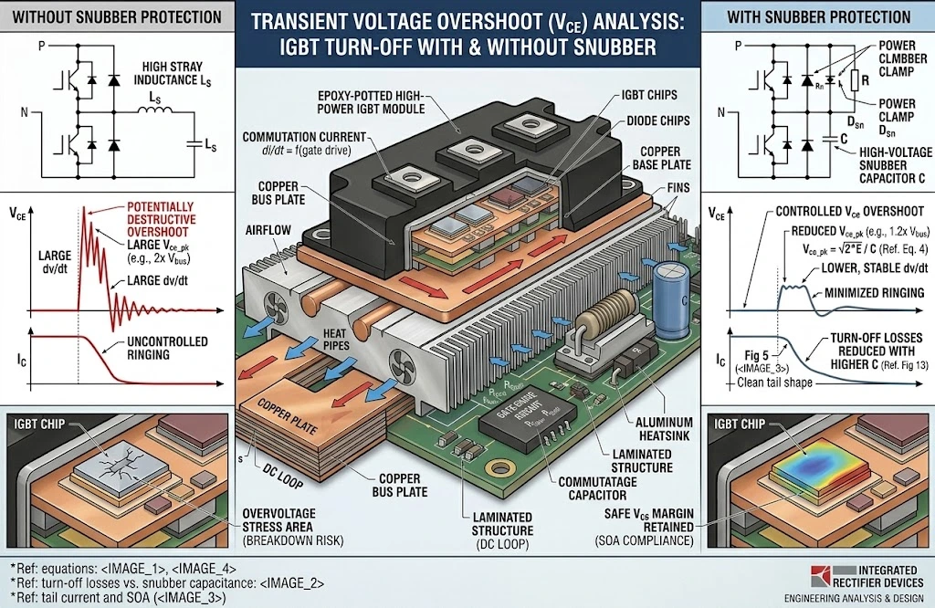
1. The Fundamental Mechanics of Voltage Overshoot and Snubber Protection
Whenever a power semiconductor turns off, the current flowing through the circuit parasitic inductance drops quickly to zero. According to Faraday’s law of induction, the induced voltage across the stray inductance is directly proportional to the magnitude of the stray inductance and the rate of current change:
Vovershoot = Lstray × (di/dt)
In high-current power modules—where total di/dt can easily reach several thousand amperes per microsecond (A/μs)—even a tiny parasitic inductance of a few tens of nanohenries (nH) produces transient voltage spikes exceeding hundreds of volts. Beyond active switch turn-off transitions, in circuits utilizing diodes with pronounced bipolar reverse-recovery characteristics, abrupt freewheeling diode snap-off during the tail of the recovery period can also excite stray-inductance ringing and contribute significantly to voltage overshoot. When stored minority carriers recombine precipitously, the resulting steep local di/dt induces high-frequency transient oscillations across the commutation loop. If the sum of the DC bus voltage (VDC) and Vovershoot exceeds the breakdown rating of the IGBT or MOSFET (VCES or VDSS), catastrophic semiconductor failure occurs.
Snubber networks mitigate this threat by introducing an auxiliary passive or active capacitive path that diverts high-frequency transient currents away from the switching device. By providing an alternate path for the current during turn-off, the snubber limits the voltage rate of rise (dv/dt) across the switch and clamps the peak voltage transient to a safe magnitude.
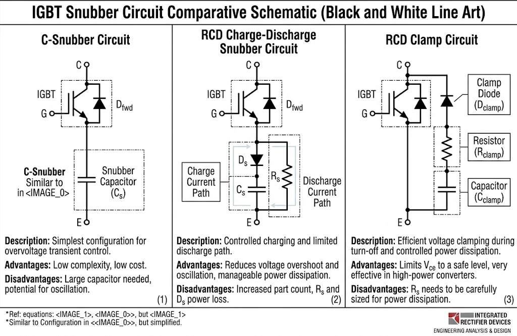
Common Snubber Topologies
Depending on power level, cost constraints, and performance requirements, engineers select from several classic snubber topologies:
- High-Frequency Decoupling Capacitors (DC-Link C-Snubbers): Connected directly across the positive and negative DC terminals of a power module. Rather than fully charging and discharging on each cycle, they function as localized, ultra-low-inductance high-frequency bypass filters that clamp commutation loop voltage spikes; their internal losses are primarily governed by capacitor ESR and ripple currents rather than cycle-by-cycle full capacitive dump. In contrast, device-level C-snubbers connected directly across individual switch terminals damp turn-off dv/dt but discharge their stored charge directly into the semiconductor channel at turn-on.
- RCD Charge-Discharge Snubbers: Utilize a diode to direct transient current rapidly into a snubber capacitor while forcing the stored capacitive energy to discharge through a resistor during the off-state or subsequent turn-on transition.
- PCD / RCD Clamp Snubbers: Clamp overvoltage transients tightly to a stable DC reference without requiring full capacitive charge-discharge cycles on every switching event.
2. The Snubber Energy Dissipation Equation: Where Efficiency Goes
To balance system protection against efficiency penalties, power design engineers must understand how snubber capacitor selection directly dictates power dissipation.
In a classical full charge-discharge snubber configuration where the snubber capacitor undergoes a complete voltage swing (ΔVswing) and subsequently dissipates that energy across a damping resistor during every switching period, the energy (Esnub) absorbed and dissipated per cycle provides an analytical upper-bound baseline loss estimate:
Esnub ≈ 0.5 × Csnub × (ΔVswing)2
Under the specific operating regime where the capacitor voltage discharges completely from the DC rail potential down to zero (ΔVswing ≈ VDC) prior to the subsequent turn-off transition, the resulting continuous dissipation penalty scales directly with the switching frequency (fsw):
Psnub_full = Esnub × fsw ≈ 0.5 × Csnub × (VDC)2 × fsw
Important Engineering Boundary: It is critical to differentiate between full charge-discharge snubbers and RCD clamp snubbers. In bridge-leg or DC-link RCD clamp configurations, the clamping capacitor is pre-biased near the DC rail voltage (VDC) and acts as an auxiliary low-impedance dynamic reservoir. Rather than repeatedly cycling its entire capacitive energy down to zero on every switching pulse, the steady-state dissipation across Rsnub is fundamentally determined by the net charge transferred during the commutation overshoot period, the clamping voltage ripple, and the steady-state bias (Vclamp2 / Rsnub). Consequently, RCD clamp networks typically yield lower continuous thermal dissipation than unconstrained charge-discharge branches, though exact dissipation must be modeled from the specific bridge topology and commutation loop parasitics.
From this equation, several technical realities become immediate:
- Frequency Scaling: Operating at higher switching frequencies to shrink magnetic components proportionally increases total snubber power loss.
- Voltage Quadratic Dependence: High DC link voltages (e.g., 800 V EV architectures or 1200 V industrial drives) drastically increase energy stored in Csnub due to the square relationship (V2).
- Capacitance Direct Scaling: Doubling Csnub directly doubles the heat dissipated in the snubber circuit per cycle.
Additionally, during turn-on, the switch must discharge the energy stored in Csnub if an unbuffered or non-damped configuration is used, creating extra switch current spikes and increasing semiconductor turn-on losses (Eon).
3. Quantifying Efficiency Sacrifices: Impact on System Thermal Budget
To visualize how snubber capacitance influences thermal overhead, consider a representative 800 V DC bus system operating at a switching frequency (fsw) of 20 kHz.
Note on Calculation Model: The values in the following matrix illustrate an idealized full charge-discharge benchmark (where the entire capacitive charge at VDC = 800 V is assumed to be dissipated every switching cycle at fsw = 20 kHz) to establish a theoretical upper-bound thermal baseline. In practice, actual continuous power losses in low-ripple DC-link bus snubbers or properly clamped RCD networks are substantially lower:
| Snubber Capacitance (Csnub) | DC Bus Voltage (VDC) | Switching Frequency (fsw) | Energy Per Cycle (Esnub) | Snubber Power Loss (Psnub) |
|---|---|---|---|---|
| 10 nF | 800 V | 20 kHz | 3.2 mJ | 64 W |
| 47 nF | 800 V | 20 kHz | 15.04 mJ | 300.8 W |
| 100 nF | 800 V | 20 kHz | 32 mJ | 640 W |
| 220 nF | 800 V | 20 kHz | 70.4 mJ | 1408 W |
In a high-power inverter rated for 100 kW, dissipating 640 W to 1408 W purely within snubber damping components accounts for 0.64% to 1.41% of the system’s baseline rated power throughput. While this proportion might initially appear modest, dissipating an incremental ~1 kW of continuous thermal overhead severely compromises thermal budgets in high-power-density designs—often requiring expanded heatsink extrusion profiles, larger liquid cold plates, or upsized cooling fans that drive up system weight and bill-of-materials (BOM) cost.
For in-depth analysis on mitigating fast di/dt transient spikes and optimizing switching transitions, refer to our comprehensive technical guide on Precision Gate Drive Design: Mastering Gate Charge and Miller Effect Mitigation.
4. Dynamic Parameter Optimization: Low Load vs. High Load (150 A vs. 350 A)
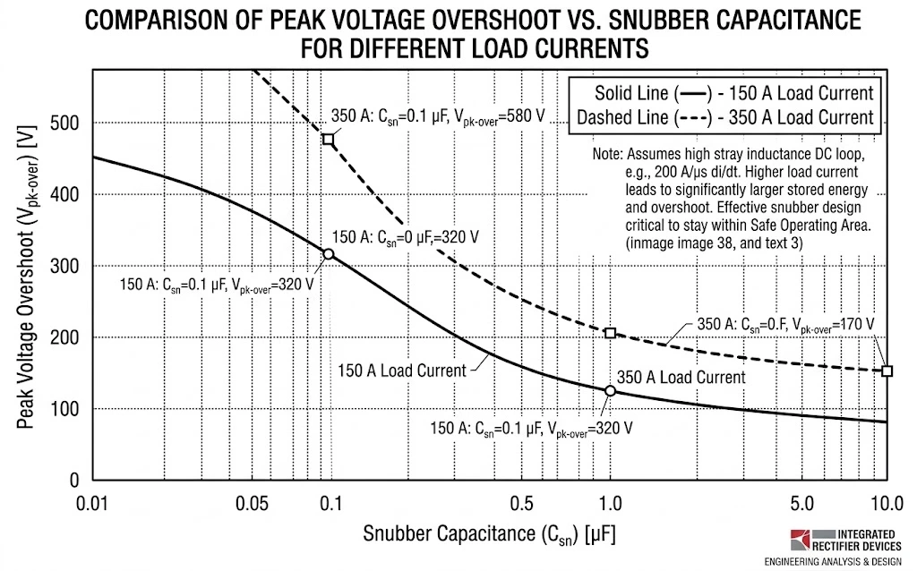
A static snubber design selected solely for worst-case operating conditions often penalizes converter efficiency across light- and medium-load ranges. Energy stored in circuit stray inductance scales with the square of the switched current (Iload):
Einductivity = 0.5 × Lstray × (Iload)2
Therefore, when switching at 350 A versus 150 A, the inductive energy that must be absorbed by the snubber network increases quadratically with load current (scaling with Iload2).
Case Study Comparison: 150 A vs. 350 A Switching Regime
Let us analyze a high-power converter operating with a total stray inductance (Lstray) of 50 nH across two distinct load current levels.
Scenario A: Moderate Load (Iload = 150 A)
For standard 150 A industrial half-bridge and six-pack converter topologies—such as those utilizing the 6MBI150VB-120-50 1200 V IGBT module:
- Stored Inductive Energy: EL = 0.5 × 50 nH × (150 A)2 = 0.5625 mJ
- Snubber Dimensioning: Because the stored inductive energy remains moderate, an illustrative starting baseline (e.g., Csnub ≈ 22 nF to 47 nF) serves as an initial bench guideline to evaluate damping response within the module’s reverse bias safe operating area (RBSOA). These values are illustrative examples rather than fixed current-based design rules; actual capacitance depends on the bus voltage, stray inductance, allowable overshoot, and selected snubber topology.
- Efficiency Consideration: An unnecessarily large 220 nF capacitor may increase switching-related losses in charge-discharge snubber configurations. Whether this capacitance is excessive must be determined from measured transient overshoot, converter switching losses, and system thermal headroom.
Scenario B: Heavy Load (Iload = 350 A to 400 A)
In heavy-duty power blocks utilizing high-current building blocks such as the FZ400R12KS4P 1200 V 400 A IGBT module:
- Stored Inductive Energy: EL = 0.5 × 50 nH × (350 A)2 = 3.0625 mJ
- Snubber Dimensioning: Switching 350 A yields over 5.4 times the trapped inductive energy compared to 150 A. Under steep turn-off transitions at 350 A, an undersized capacitor may permit excessive voltage overshoot; the actual peak surge must be established from the selected circuit topology and verified through double-pulse testing.
- Optimization Baseline: A larger capacitance range (e.g., 100 nF to 220 nF) serves as an illustrative empirical starting baseline to guide bench evaluation (likewise an illustrative guideline rather than a current-based rule, as true requirements vary with bus voltage, stray inductance, and overshoot targets). However, the exact capacitance requirement must never be arbitrarily assumed; switching overshoot must be validated through double-pulse testing (DPT) across relevant junction temperature ranges (Tvj_op), while short-circuit turn-off withstand capability must be evaluated separately using dedicated short-circuit characterization procedures. The resulting thermal dissipation (Psnub) is an engineering trade-off required to guarantee device survival under maximum overload conditions.
5. Snubber Capacitors: Material Selection and Parasitic Requirements
Choosing the correct capacitance value (Csnub) is only half the engineering challenge. The physical construction and dielectric material of the snubber capacitor play an equally critical role in transient clamping effectiveness and thermal survival.
Film Capacitors vs. Multi-Layer Ceramic Capacitors (MLCCs)
Snubber capacitors are subjected to extreme pulsed currents (high dV/dt and dI/dt) during every switching event. The two primary dielectric choices are Polypropylene Film and High-Voltage C0G/NP0/X7R Ceramic Capacitors:
- Metallized Polypropylene Film Capacitors (MKP): The definitive industry standard for high-power IGBT and thyristor snubbers. Premium pulse-grade film capacitors—epitomized by dedicated high-end series such as WIMA Snubber MKP / Snubber FKP, alongside pulse-rated offerings from TDK/EPCOS and KEMET—provide proven self-healing properties, exceptionally low dielectric dissipation factors (tan δ), and negligible capacitance degradation under continuous DC bias voltage. Designers should verify the manufacturer’s specific series datasheet to confirm peak pulse current handling, maximum dV/dt limits, ESR, and internal temperature rise constraints, as internal electrode architectures and ratings differ substantially across MKP and FKP constructions. Designers must always consult the manufacturer’s specific datasheet for exact dV/dt ratings (which vary substantially based on electrode metallization, pitch, and lead terminations) and verify that peak repetitive current (Ipeak) and RMS current ratings (Irms) satisfy converter operating limits.
- Class I C0G / NP0 Ceramic Capacitors: Feature virtually zero DC-bias voltage coefficient, minimal dielectric losses, and ultra-low ESL. Although their volumetric capacitance density is lower, they represent a suitable option for localized ultra-high-frequency ringing suppression on compact SiC/GaN gate drivers and low-power bridge configurations when voltage, capacitance, and pulse-current ratings meet the application requirements.
- Class II Ceramic Capacitors (e.g., X7R, X8R): Require extreme caution in high-voltage snubber applications. Because of the ferroelectric nature of barium titanate dielectrics, Class II capacitors suffer from pronounced DC-bias capacitance loss. Depending on the applied electric field intensity (V/μm) and package form factor, the effective capacitance at nominal bus voltage can drop substantially (frequently by 40% to 75% relative to zero-bias nameplate value), potentially undermining overvoltage clamping margins unless explicitly derated against manufacturer bias curves.
Minimizing Internal and External Loop Inductance
A snubber capacitor cannot clamp a rapid voltage overshoot if the PCB traces or connecting busbars introduce additional parasitic inductance (Lsnubber_loop). If the snubber loop inductance is high, the initial voltage spike will occur before current can physically enter the snubber capacitor.
To achieve optimal performance:
- Integrate planar laminated busbars directly across the DC link. In industrial variable frequency drives (VFD) and servo converters, closely-spaced parallel conductive plates separated by thin dielectric insulation maximize mutual magnetic flux cancellation, compressing typical commutation loop stray inductance from 80–120 nH down to 15–30 nH, thereby directly relieving the capacitance sizing and thermal burden on external snubbers.
- Mount C-snubbers or dedicated snubber modules directly across the power module terminal lugs with minimal interconnecting lead length.
- Keep loop trace length as short and wide as possible on printed circuit boards.
- Select low-ESL pulse-rated film capacitors engineered specifically with direct-mount lug terminals.
For practical methodologies on integrating power modules with optimal thermal heatsinks and low-inductance busbars, explore our architectural white paper on IGBT Design & Integration: Gate Drive, Thermal Management & Circuit Topologies.
6. Practical Step-by-Step Snubber Parameter Calculation Guide
To systematically calculate the minimum required snubber capacitor (Csnub) and snubber resistor (Rsnub) for a given power stage, engineers can follow this standard analytical workflow:
Step 1: Determine Total Loop Stray Inductance (Lstray)
Measure or estimate the total parasitic loop inductance using double-pulse testing or 3D electromagnetic field simulation. A typical high-power IGBT half-bridge assembly features Lstray between 20 nH and 100 nH.
Step 2: Define Maximum Allowable Voltage Overshoot
Set the target maximum peak collector-emitter voltage (VPK). Select a project-specific voltage margin based on the device breakdown ratings (VCES), DC-link operating range, switching conditions, applicable reliability requirements, and measured transient results. Verify the maximum peak voltage under worst-case operating conditions rather than relying on a universal percentage of VCES:
ΔVmax = VPK – VDC
Step 3: Calculate Snubber Capacitance (Csnub)
The required snubber capacitance depends heavily on the chosen circuit topology and whether the capacitor is pre-biased at the DC bus potential:
- Pre-Biased RCD Clamp Configuration: When the clamping capacitor is pre-charged to the DC rail voltage (VDC) and absorbs only the inductive surge from VDC up to VPK, the energy balance equation accounts for initial voltage storage:
0.5 × Lstray × (Imax)2 = 0.5 × Csnub × (VPK2 – VDC2)
Solving for minimum capacitance yields:
Csnub ≥ (Lstray × Imax2) / (VPK2 – VDC2) - Idealized Zero-Bias Resonant Approximation: In basic unbuffered resonant damping branches where the initial capacitor voltage is zero and the full transient excursion is approximated by ΔVmax, engineers sometimes reference the first-order estimation:
Csnub_est ≈ (Lstray × Imax2) / (ΔVmax)2
Important Application Boundary: Because this simplified formula assumes zero initial charge, it does not accurately represent pre-biased DC-link clamp circuits. For pre-charged RCD clamp architectures, designers should prioritize the full energy-balance equation above and confirm final capacitance requirements via double-pulse testing (DPT).
Apply an appropriate design margin based on capacitor tolerance, temperature characteristics, operating voltage, and the empirical results of double-pulse testing.
Step 4: Dimension the Snubber Resistor (Rsnub) and Thermal Rating
The snubber resistor selection is fundamentally governed by the specific circuit topology and the operational compromise between capacitive reset timing and semiconductor stress:
- Topology-Dependent Reset Time: In classical charge-discharge networks where the snubber capacitor must discharge before the subsequent turn-off cycle, Rsnub must permit sufficient reset within the available minimum on-time (ton_min). If three time constants (3τ = 3 × Rsnub × Csnub) are allocated for near-complete reset:
Rsnub ≤ ton_min / (3 × Csnub)
Note for Clamp Architectures: In RCD clamp topologies, the capacitor is not discharged to zero each cycle; instead, the discharge time constant is engineered to span multiple switching periods (Rsnub × Csnub ≫ 1/fsw) to maintain a relatively smooth clamping voltage rail with minimal ripple.
- Turn-On Peak Current Limiting: In unbuffered circuits, selecting Rsnub too low causes an aggressive capacitive discharge current spike (Ipk ≈ VDC / Rsnub) into the semiconductor channel at turn-on, increasing switch turn-on energy (Eon) and risking latch-up.
- Continuous Power & Pulse Energy Derating: Always select a non-inductive thick-film or ceramic composition resistor. The required continuous power rating (Prated) must be determined by derating against the manufacturer’s thermal datasheet for the specific heatsink mounting thermal resistance and ambient airflow, ensuring adequate safety margin above actual continuous dissipation while verifying single-pulse energy absorption capability (Joules/pulse) under repetitive switching surges. Detailed calculation principles are outlined in standard design literature such as Texas Instruments SLPA010: Snubber Circuits Theory, Design and Application.
7. Engineering Trade-Off Matrix: Protection vs. Efficiency
Designing an optimized snubber system requires balancing conflicting engineering priorities. The summary matrix below outlines how varying design parameters influences circuit performance:
| Design Action | VCE Peak Overshoot | dv/dt & EMI Noise | Snubber Dissipation (Ploss) | Switch Turn-On Stress |
|---|---|---|---|---|
| Increase Capacitance (Csnub) | Significantly Decreased | Improved (Lower dv/dt) | May increase (dependent on topology, voltage swing, switching frequency, and energy recovery path) | Higher peak current spike |
| Decrease Capacitance (Csnub) | Increased (Higher risk) | Worse (Higher dv/dt) | May decrease (subject to topology and operational boundaries) | Lower turn-on current stress |
| Reduce Stray Inductance (Lstray) | Significantly Decreased | Improved | Decreased (Allows smaller C) | No negative impact |
| Increase Resistance (Rsnub) | Higher initial clamp peak | Damped oscillations | Shifted heat to resistor | Incomplete C discharge |
8. Summary and Design Recommendations for Junior Engineers
Snubber networks remain an essential tool in high-power converter design, offering effective protection against voltage transients and extending device operational life. However, snubber capacitor selection should never be based on arbitrary rules of thumb. Increasing snubber capacitance can increase switching-related losses, particularly in charge-discharge networks. The actual loss depends on the snubber topology, voltage swing, switching frequency, and energy recovery path.
For junior engineers and power designers developing next-generation converters, follow these primary design takeaways:
- Prioritize Layout First: Always minimize physical loop inductance (Lstray) through tight PCB layout and laminated busbars before sizing snubber components. Lowering Lstray reduces the required Csnub value without sacrificing safety margin.
- Tailor to Real Load Profiles: Optimize Csnub based on realistic maximum load current levels (e.g., distinguishing between 150 A continuous and 350 A transient peak regimes) to avoid over-designing the capacitive damping network.
- Account for Dielectric Loss: Always select low-ESR metallized polypropylene film or high-voltage C0G ceramic capacitors for high dV/dt pulse environments to prevent internal dielectric overheating.
- Validate Thermal Ratings: Ensure snubber resistors are adequately heatsunk or derated to handle continuous cyclical thermal dissipation.
By carefully balancing snubber capacitor selection against efficiency losses, engineers can build high-power converters that achieve both maximum reliability and peak energy efficiency. To review engineering application notes, module datasheets, and replacement portfolios across global power converter platforms, consult the technical resources in our Power Electronics Masterclass: The Definitive Guide to IGBT Selection & System Reliability.