
Stray Inductance, Transient Voltage Overshoot, and Snubber Network Design in IGBT and MOSFET Power Stages
In modern high-frequency power electronics, power semiconductor switches such as Insulated Gate Bipolar Transistors (IGBTs) and Metal-Oxide-Semiconductor Field-Effect Transistors (MOSFETs) are routinely operated at steep switching speeds (di/dt exceeding 1000 to 5000 A/μs) to minimize turn-off switching energy dissipation (Eoff). However, aggressive turn-off current slopes combined with parasitic magnetic energy trapped in the commutation loop give rise to severe dynamic electrical stress across the semiconductor junction. Stray inductance, coupled with high rates of current fall, generates localized transient voltage overshoot spikes that threaten device dielectric breakdown and degrade electromagnetic compatibility (EMC).
Addressing these high-voltage transients requires a structured engineering hierarchy that combines low-inductance packaging, high-frequency bus decoupling, tailored passive snubber networks, and active gate clamp mechanisms.
Quantifying Transient Voltage Overshoot from Stray Inductance
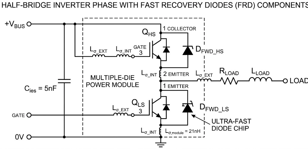
Every electrical conductor within a converter physical architecture—including internal bond wires, module power terminals, laminated DC busbars, and filter capacitor banks—exhibits parasitic stray loop inductance (Lσ). Internal module package inductance typically contributes 10 nH to 30 nH, while external busbars and DC-link connections contribute an additional 20 nH to 80 nH. During switch turn-off, current flowing through the device falls rapidly from its operating value to zero within tens to hundreds of nanoseconds.
The induced transient voltage spike across the collector-emitter (VCE) or drain-source (VDS) terminals is governed by Faraday’s law of induction:
Vpeak = VDC + Vovershoot = VDC + Lσ × (di/dt)
For an illustrative calculation, assume a nominal DC bus voltage of 340 V, a turn-off current slope of 3000 A/μs, and a total commutation-loop inductance of 50 nH:
di/dt = 3000 A/μs = 3 × 10⁹ A/s
Vovershoot = (50 × 10-9 H) × (3 × 10⁹ A/s) = 150 V
Adding this calculated overshoot to the 340 V working DC bus results in a peak terminal voltage of 490 V. In high-power industrial inverters operating from 600 V to 800 V DC buses, or during hard overcurrent and desaturation turn-off where di/dt escalates, peak voltage transients can easily exceed the device’s maximum repetitive peak collector-emitter rating (VCES). Furthermore, the reverse recovery current (Irr) and snappy snap-off characteristics (direc/dt) of the freewheeling diode induce secondary high-frequency ringing that amplifies peak overvoltage stress across high-current switches such as the 1MBI900V-120-50 power module.

First-Line Suppression: Bus Layout, Decoupling, and Kelvin Emitter
Before implementing auxiliary secondary clamping circuits, primary converter design must focus on minimizing the total commutation loop inductance (Lσ). Industrial hardware achieves low-inductance performance through three fundamental techniques:
- Laminated Low-Inductance Busbars: Overlapping positive and negative planar DC conductors with thin dielectric insulation (such as polyimide or Nomex) maximizes mutual magnetic flux cancellation, reducing busbar parasitic inductance to single-digit nanohenry ranges.
- Direct-Mount Film Decoupling Capacitors: Low equivalent series inductance (ESL < 15 nH) polypropylene film snubber capacitors are placed directly across the DC module terminals. These components provide a localized, low-impedance AC current bypass during switching, shielding the main DC-link bulk capacitors from high-frequency current harmonics.
- Dedicated Kelvin Emitter (Auxiliary Emitter) Routing: Sharing the power emitter terminal between the main collector-emitter current path and the gate-emitter drive loop introduces common emitter inductance (LE). The rapid di/dt induces an opposing voltage drop (VLE = LE × di/dt) that reduces effective gate drive voltage during turn-on and causes gate voltage oscillation during turn-off. Modern high-power IGBT modules feature a dedicated Kelvin emitter terminal that separates gate return current from power commutation loops, as detailed in our guide on internal module packaging and bond wire layout.
Passive Snubber Circuit Architecture and Initial Sizing Guidelines
When physical layout optimization and local decoupling capacitors cannot bring transient voltage spikes below targeted safe margins (typically ≤ 80% of VCES), engineers install passive snubber networks. Snubber circuits absorb the trapped magnetic energy stored in the parasitic loop inductance and damp transient oscillations.
RC vs. RCD Clamp Snubber Topologies
Passive snubber networks generally employ one of two configurations:
- RC Snubber: A simple series resistor-capacitor network connected across collector-emitter terminals. It provides bidirectional damping, making it effective for suppressing high-frequency diode reverse recovery ringing. However, it incurs continuous power dissipation during both turn-on and turn-off transitions.
- RCD Clamp Snubber: Incorporates a fast-recovery steering diode (Ds), a snubber capacitor (Cs), and a discharge resistor (Rs). The operational behavior and energy release loop depend directly on whether the network is configured as a DC-link bus clamp or an individual switch clamp:
- DC-Link RCD Clamp: Connected directly across the positive and negative DC rails near the module. During turn-off overshoot, diode Ds conducts, routing inductive current into Cs. The trapped charge then discharges through Rs back into the DC-link bus, converting peak overshoot energy into resistive heat.
- Individual Switch RCD Snubber: Connected in parallel with each switch. The diode charges Cs during turn-off to clamp dv/dt and VCE. During the switch’s subsequent on-state (ton), Cs discharges through Rs and the conducting IGBT channel, dissipating the stored charge primarily as heat inside Rs.
For complex converter systems, foundational design equations and layout topologies are comprehensively detailed in our sister reference on stray inductance and snubber design across high-frequency converters as well as established technical treatises on passive snubber circuit networks.
Baseline Component Dimensioning and Boundary Conditions
To establish an initial baseline for snubber capacitance (Cs), engineers often use an energy-balance relationship assuming an idealized DC-link RCD clamp where the capacitor initial voltage equals VDC and all inductive energy is transferred into Cs:
Cs ≥ (Lσ × Ipeak2) / (ΔV × (2 × VDC + ΔV))
Applicability Notes: This expression represents a simplified first-order design estimate. Actual required capacitance depends on the specific circuit topology (DC clamp vs. individual switch snubber), the initial pre-charge voltage of Cs, reverse recovery energy from freewheeling diodes, and power source contribution during commutation. Final capacitor selection must be validated using physical double-pulse test waveforms under maximum fault conditions.
The discharge resistor (Rs) provides a reset path so that Cs returns close to its baseline voltage before the next turn-off transient occurs. Using a three-time-constant rule (3τ) provides an initial guideline where the transient voltage delta ΔV decays by approximately 95%:
Rs ≤ ton,min / (3 × Cs)
Boundary Notes: The 3τ relationship is a rule-of-thumb estimate. For systems operating at narrow on-time pulses (low duty cycles) or requiring higher reset precision, the discharge timing must be strictly calculated using Rs ≤ -ton,min / (Cs × ln(ε)), where ε is the acceptable fractional residual voltage overshoot.
Furthermore, the power dissipation rating of Rs depends heavily on the chosen topology and voltage swing:
- For a DC-link clamp snubber where Cs only charges and discharges over the overshoot window ΔV, resistor power loss is approximately:
PRs ≈ 0.5 × Cs × (ΔV)2 × fsw - For an individual switch snubber where Cs fully discharges from VDC + ΔV to near 0 V during each on-state, total energy per cycle is substantially higher:
PRs ≈ 0.5 × Cs × (VDC + ΔV)2 × fsw
Always select non-inductive thick-film power resistors mounted on suitable heatsinks to avoid introducing parasitic series inductance into the clamp loop. Detailed layout verification tables are cataloged in the Fuji Electric IGBT Module Application Manual on Snubber Design.
Active Clamping Networks and Gate Driver Dynamics
Active clamping provides a dynamic, gate-level voltage limiting mechanism that suppresses collector-emitter voltage transients without requiring bulky, high-wattage passive snubber resistors. In an active clamping topology, a series chain of transient voltage suppressor (TVS) or Zener diodes is connected directly between the collector and gate terminals of the IGBT.
When dynamic turn-off overvoltage forces VCE above the TVS breakdown voltage (VZener), avalanche current (Iclamp) injects into the gate node. This injected current counteracts the gate driver pull-down current, holding the gate-emitter potential (VGE) in the active linear amplification region. By partially conducting collector current, the switch slows the overall di/dt rate of fall.
Dynamic Clamping Voltage and Circuit Dependencies
The actual clamping voltage (Vclamp) is not a fixed scalar constant and cannot be simplified to a basic static sum. Instead, it is governed by a dynamic feedback loop:
Vclamp(t) = VTVS(Iclamp, Tj) + Iclamp × RG,sink + VGE(active)(IC, Tj)
Where:
- VTVS: The breakdown voltage of the TVS chain, which increases with instantaneous avalanche current (dynamic resistance Rdyn) and operating junction temperature.
- RG,sink: The gate driver turn-off pull-down impedance, across which clamp current creates an additional offset voltage.
- VGE(active): The gate-emitter voltage required to support instantaneous collector current IC according to the IGBT transfer characteristics.
Design Trade-offs and Thermal Stress
While active clamping provides effective protection against unexpected load dumps and short-circuit turn-off transients, it forces the semiconductor die to dissipate the trapped inductive magnetic energy directly as internal junction heat:
Eclamp = ∫ (VCE(t) × IC(t)) dt
Repeated active clamping cycles during high-frequency switching can quickly exceed the maximum junction temperature (Tj,max = 150°C or 175°C), resulting in thermal runaway. Therefore, active clamping is primarily deployed as a fail-safe emergency clamp rather than a continuous steady-state snubber.
For robust gate drive implementation, active clamping is typically integrated alongside advanced desaturation (DESAT) fault detection and active Miller clamping. Detailed gate charge dynamics and circuit topologies are explored in our guide on precision gate drive design and Miller clamp strategies and negative off-bias gate drive implementations. Component engineers can also consult the Infineon 1200V HighSpeed IGBT Switching Dynamics & Gate Sizing Guide and examine certified galvanic isolated gate driver ICs.
Double-Pulse Test (DPT) & Physical Validation Workflow
To validate switching transients and verify that peak voltage spikes remain within safe operating limits, power electronics engineers utilize a Double-Pulse Testing (DPT) workflow:
- Parametric Characterization Across SOA: Configure test current levels and junction temperatures strictly within the safe operating boundaries defined by the manufacturer’s Reverse Bias Safe Operating Area (RBSOA). For robust industrial modules rated for inductive turn-off, characterization typically evaluates currents up to the rated pulse or RBSOA ceiling (which can extend up to 2 × IC,nom for ruggedized IGBTs) across ambient to maximum junction temperatures (25°C to 150°C/175°C). Pulse durations must be strictly controlled to prevent excessive junction heating.
- Empirical Stray Inductance Extraction: Calculate the effective commutation loop inductance from measured transient waveforms using the relation Lσ ≈ Vovershoot / (di/dt).
- Measurement Integrity: Use high-voltage differential probes with low input capacitance and calibrated Rogowski coils or coaxial current shunts. Keep ground leads as short as possible to prevent electromagnetic field pickup from distorting fast dv/dt (> 10 kV/μs) signals.
- Fault Protection Validation: Verify active clamp response and gate driver desaturation blanking times during hard switching faults (HSF) and fault-under-load (FUL) conditions to ensure peak terminal voltages remain securely below datasheet absolute maximum ratings.
Industrial Power Component Sourcing & Engineering Support
Mitigating transient voltage overshoot requires pairing sound circuit design with certified, high-reliability power semiconductors. As an independent distributor with over 15 years of industry experience, Shunlongwei Co. Ltd. maintains an extensive global inventory of genuine IGBT modules, SiC power stages, fast recovery diodes, and DC-link film capacitors from leading manufacturers. Whether sourcing standard industrial modules or seeking replacements for urgent production lines, contact our engineering sales team for rapid RFQ processing and complete traceability verification.