


Content last revised on September 10, 2026
Symmetrical Busbar Geometry for High-Current Parallel Module Arrays
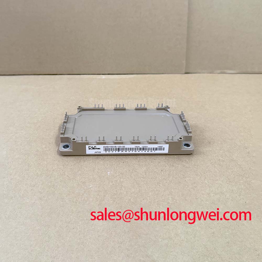
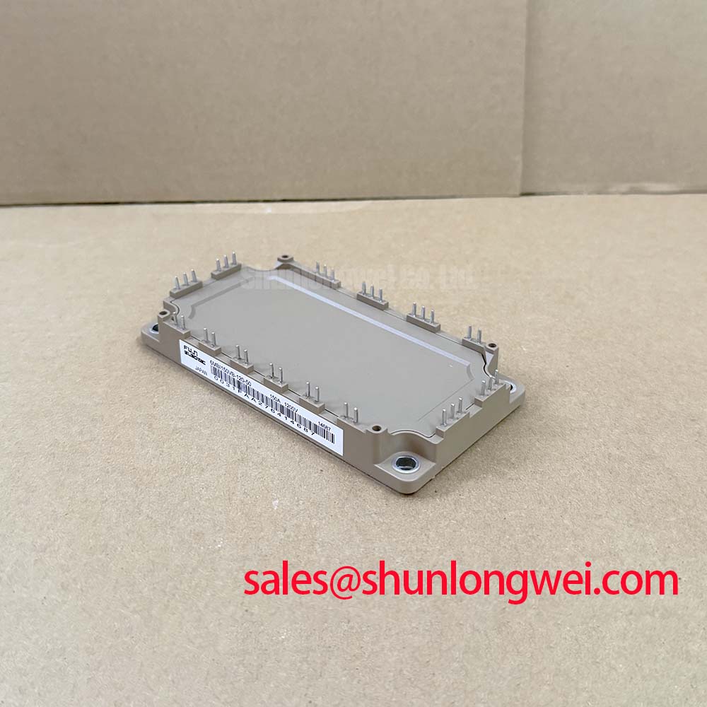
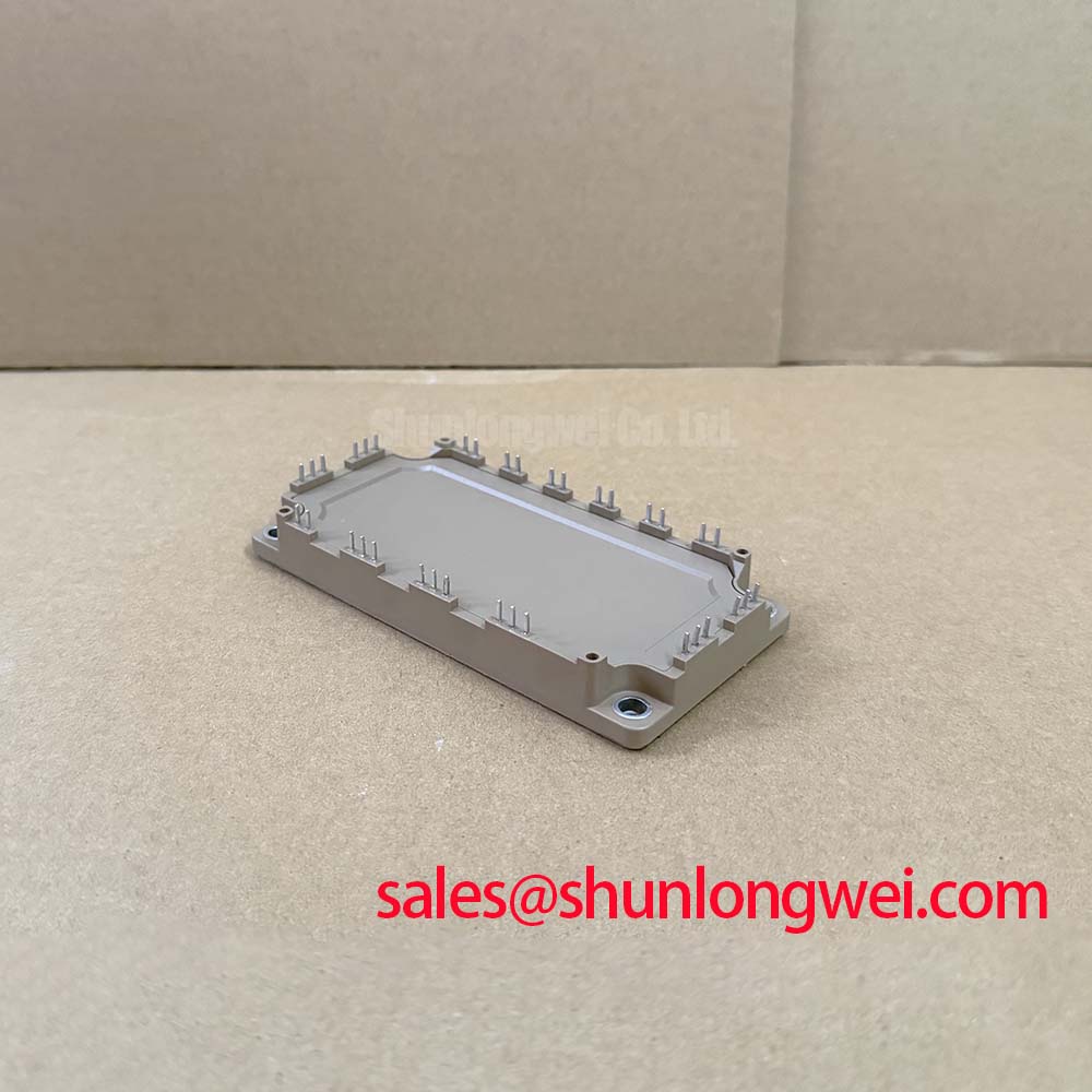
Incoming inspection of six-pack power stages destined for industrial material handling and electric forklift traction inverters begins with static characterization at the test bench. When evaluating the 6MBI150VB-120-50, incoming quality verification focuses on screening terminal saturation voltage against chip-level behavior. Factory documentation specifies a typical chip saturation voltage of VCE(sat) = 1.75 V at Tj = 25°C, whereas terminal measurements yield VCE(sat) = 2.50 V (Official Datasheet Specification) under full load due to the internal bond wire and pin resistance. In multi-module traction drives requiring paralleled bridge legs, the positive temperature coefficient of VCE(sat) at elevated junction temperatures provides intrinsic steady-state current balancing, but physical layout symmetry remains non-negotiable for dynamic sharing.
During bench static testing, cold-state forward voltage matching across all six internal switches is evaluated using a calibrated four-wire Kelvin test fixture. When engineers parallel dual three-phase inverters to handle heavy mast lifting or high-torque ramp ascents, unbalances during switching transitions originate primarily from asymmetric trace inductances rather than chip-to-chip variations. Symmetrical busbar geometry demands identical conductor path lengths, matched clearance planes, and dedicated auxiliary emitter connections. By separating the main power return path from the gate signal return using the integrated Kelvin emitter auxiliary terminals, gate drive circuits avoid spurious induced voltages caused by high di/dt load currents through the emitter bond wires.
| Parameter | Symbol | Rated Value (Datasheet Spec) | Incoming QA Verification Method |
|---|---|---|---|
| Collector-Emitter Voltage | VCES | 1200 V | Static leakage current test at VGE = 0 V, ICES < 1.0 mA |
| Continuous Collector Current | IC | 150 A (at Tc = 100°C) | Thermal chamber steady-state conduction verification |
| Pulsed Collector Current | ICP | 300 A (1 ms, Tc = 80°C) | Single-pulse transient short-circuit bench screening |
| Input Capacitance | Cies | 13.7 nF (f = 1 MHz) | LCR bridge measurement across G-E terminals |
| Isolation Voltage | Viso | 2500 VAC (1 minute) | Dielectric withstand test between terminals and baseplate |
To monitor current symmetry across high-stress parallel branches, external diagnostic loops often integrate isolated hall sensors or differential shunt monitors like ADI High Precision Current Sense Amplifiers directly onto the phase output busbars. For heavy-duty industrial vehicles requiring significantly higher current handling beyond the continuous 150 A rating of this unit, the related 6MBI450V-170 provides a higher current capacity option within a compatible architectural philosophy.
Baseplate Thermal Grease (TIM) Layer Control & Heatsink Mounting Torque Optimization
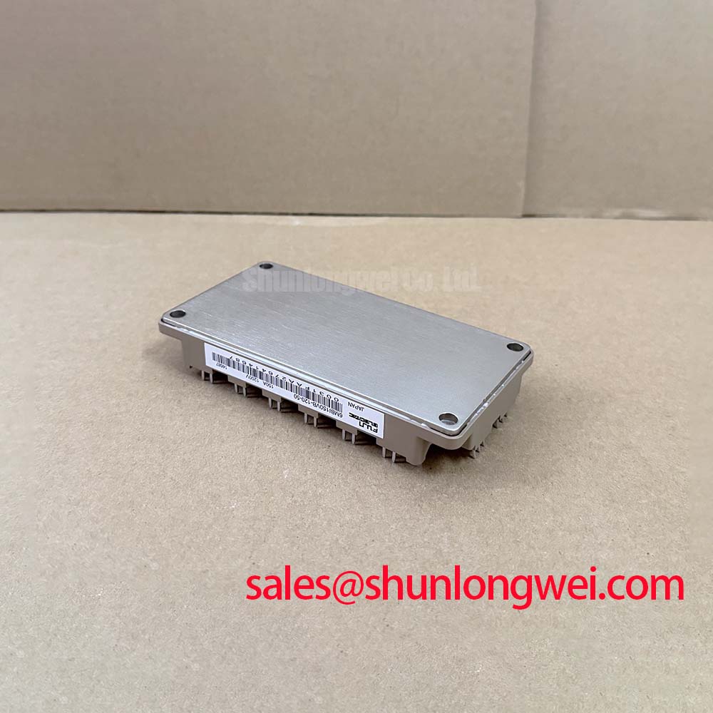
Thermal management evaluation on incoming modules focuses on baseplate planarity and interfacial thermal resistance. The copper baseplate of the 6MBI150VB-120-50 exhibits a slight factory-engineered convex bow, designed to flatten against the heatsink under uniform fastener load. Installing the module without precise thermal interface material (TIM) thickness control leads to air voids, high localized thermal impedance, and premature thermal runout during steep forklift acceleration profiles.
Applying TIM through a precision stainless-steel mesh screen yields a controlled wet thickness between 50 µm and 100 µm across the clean aluminum or copper cold plate. When the module is placed onto the thermal compound, fastening must follow a crosswise tightening sequence: initially seating all M5 mounting screws finger-tight to approximately 1.0 N·m, followed by a final calibrated tightening to 2.5–3.5 N·m (General Industry Design Consideration for M5). This sequence prevents tilting the internal direct bonded copper (DBC) substrate, ensuring even grease expulsion toward the module perimeter.
💡 Bench Tip: Before applying thermal compound or placing the module into a heatsink fixture, ground your wrist strap to an ESD workstation and perform a diode-mode check across all free-wheeling diode (FWD) pairs. The forward voltage drop VF at room temperature should read between 0.35 V and 0.55 V on standard digital multimeters. Any gate terminal showing leakage or an erratic VGE(th) threshold during pre-installation checks indicates electrostatic gate rupture, requiring immediate component quarantining.
From an overcurrent and fault clearance perspective, coordination with high-speed semiconductor fuses is essential. The peak pulsed collector current rating of ICP = 300 A defines the boundary for short-duration overload before desaturation protection or fast-acting I2t fuse elements isolate the DC bus, safeguarding the DBC ceramic against thermal cracking.
DC-Bus Operating Voltage Headroom Derating for Single Event Burnout (SEB) Immunity
Equipment deployed in automated high-bay warehouses or mountainous logistics distribution centers above 2000 meters altitude experiences elevated terrestrial neutron flux compared to sea-level operations. Power semiconductors operating near their breakdown limits face increased vulnerability to catastrophic Single Event Burnout (SEB), where a single high-energy neutron triggers a localized avalanche plasma track through the silicon drift region.
Although the module carries an official breakdown specification of VCES = 1200 V, standard traction design practice requires deep DC-bus voltage headroom derating. In 400 VAC to 480 VAC line-fed systems or battery-buffered traction buses, nominal DC-link voltages are routinely restricted to 600 V to 750 V under steady-state conditions. Operating at this reduced voltage level provides exponential reductions in cosmic ray failure-in-time (FIT) rates, ensuring high mean time between failures under harsh duty cycles.
Incoming quality assurance protocols evaluate baseplate-to-substrate dielectric insulation integrity using standardized high-potential test benches. Verifying the dielectric boundary rated at Viso = 2500 VAC for 60 seconds ensures no micro-void partial discharge occurs along the internal potting silicone gel. For testing methodology, insulation derating standards, and diagnostic procedures applicable to field repair, refer to the Field Engineer’s Handbook for comprehensive failure analysis techniques.
DC-Bus Low-Inductance Laminated Busbar Design & Turn-Off Voltage Overshoot Suppression
During hard turn-off at rated current, the rate of current decay di/dt across the IGBT channel interacts with the stray parasitic inductance of the internal module leads and external busbar assembly. This inductive energy produces an instantaneous terminal voltage spike defined by the dynamic relationship where total peak turn-off voltage equals the nominal DC bus potential plus the product of stray inductance and di/dt. If this peak transient exceeds the rated VCES of 1200 V, immediate dielectric breakdown of the silicon collector junction occurs.
Minimizing this transient requires planar laminated busbars where positive and negative copper conductor plates are interleaved with thin dielectric films (such as 0.25 mm Nomex or Kapton), creating wide, parallel mutual coupling paths. This construction targets a total loop inductance below 25 nH. Close-coupled polypropylene film snubber capacitors positioned directly across the DC terminal pins absorb residual inductive energy, effectively clamping high-frequency voltage ringing.
Static capacitance verification at the bench involves measuring the input capacitance Cies = 13.7 nF at 1 MHz (Official Datasheet Specification). Bench technicians verify that the gate charge profiles correlate with drive circuit impedance requirements. Sizing the series gate resistor determines the turn-off commutation speed, providing bench-level control over transient di/dt to maintain safe turn-off trajectories well within the Reverse Bias Safe Operating Area (RBSOA) boundary at maximum operating junction temperatures up to Tjop = 150°C.