Content last revised on September 10, 2026
Optocoupler vs Digital Coreless Transformer Isolation in High-Voltage Switching
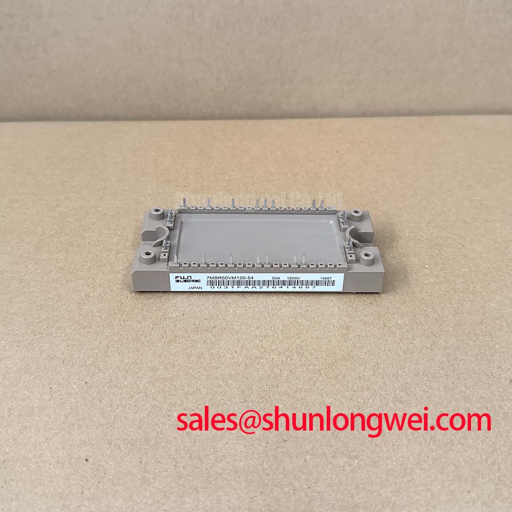
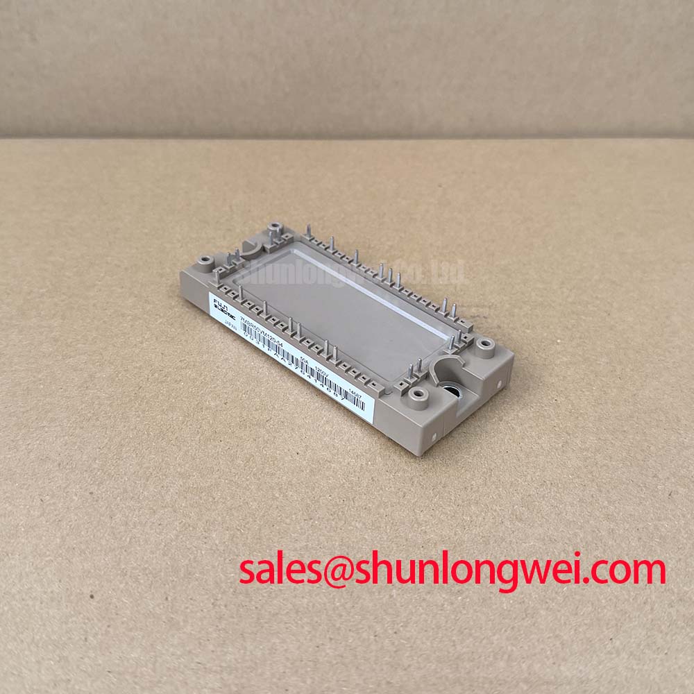
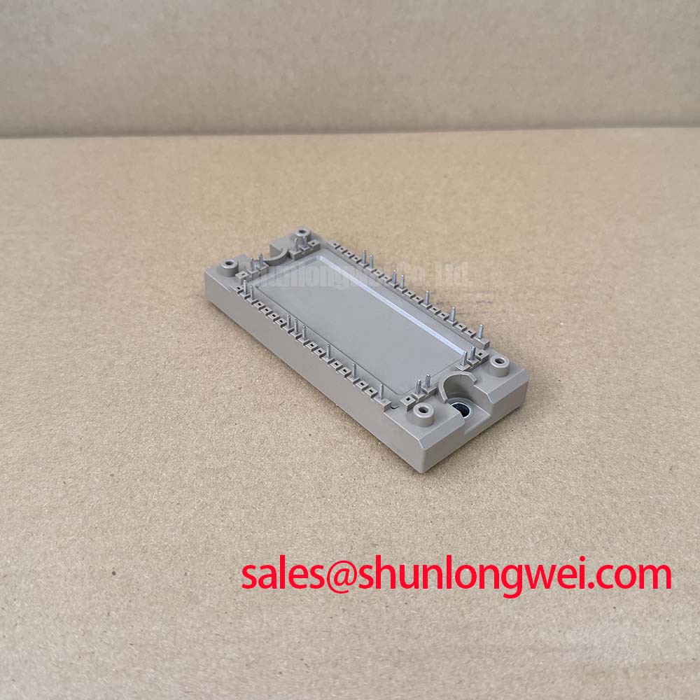
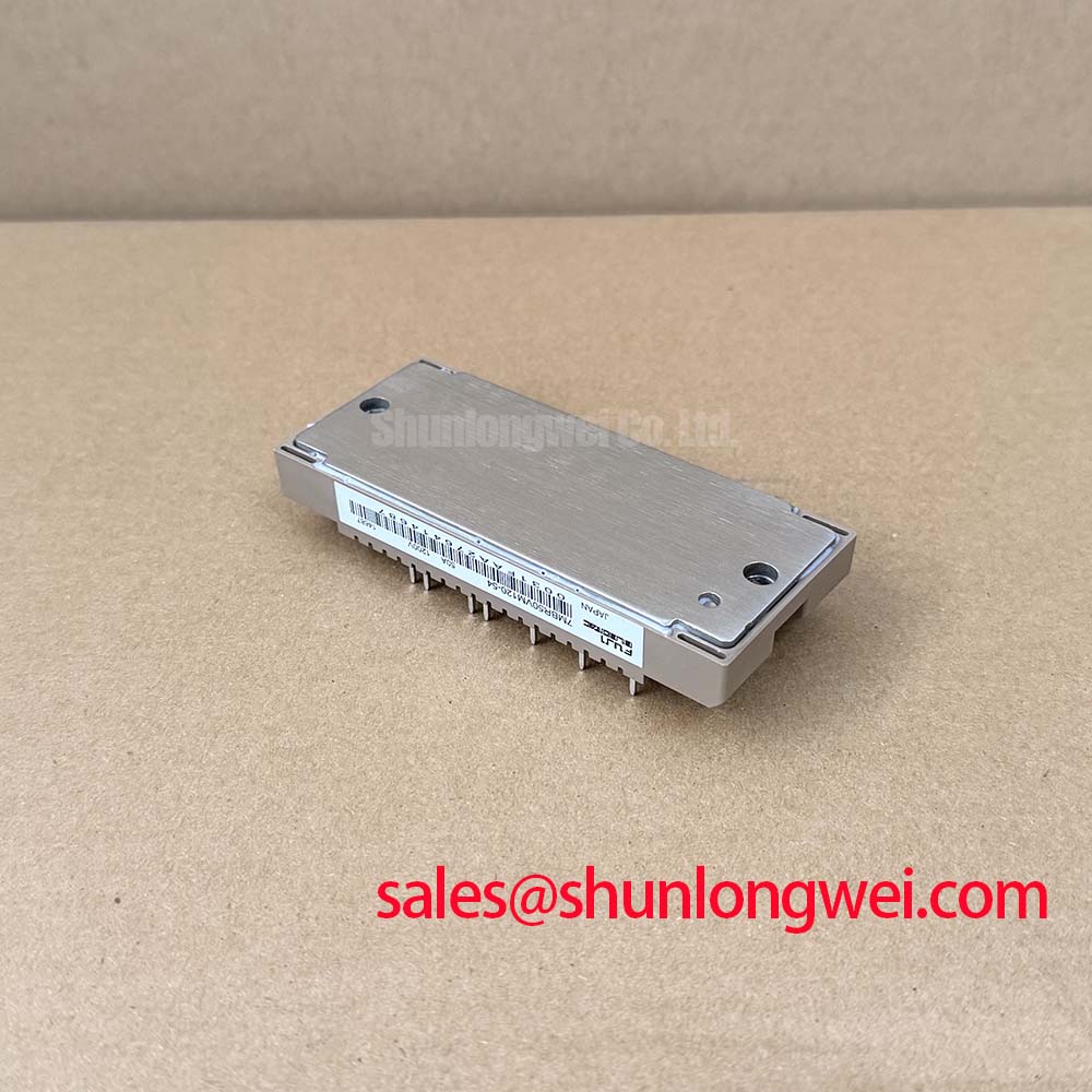
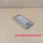
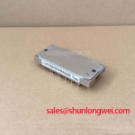
Operating a wind turbine pitch and yaw converter at altitudes exceeding 3,000 meters subjects power electronics to extreme physical stressors: rarefied air with reduced dielectric breakdown strength, severe thermal cycling between -40°C and +85°C nacelle ambient, and elevated cosmic ray neutron flux. When an emergency field triage call comes in for an unexpected pitch drive inverter trip on a 2.5 MW turbine, the power stage is the first point of inspection. The Fuji Electric 7MBR50VM120-54 integrates a full seven-pack PIM (Power Integrated Module) topology—comprising a three-phase input rectifier, a three-phase inverter bridge rated at VCES = 1200V and continuous IC = 50A (TC = 80°C) (Official Datasheet Specification), and an integrated dynamic braking chopper. Controlling these IGBT gates reliably under steep switching transients requires a robust galvanic isolation boundary.
Field technicians troubleshooting gate driver boards frequently encounter spurious gate triggering caused by common-mode ground bounce. During high-speed switching events, the inverter phase leg experiences voltage gradients exceeding 15 kV/µs. Standard optocouplers with internal LED-photodiode arrangements often suffer from parasitic coupling capacitance across their isolation barrier (typically 0.6 pF to 1.5 pF). This capacitance allows common-mode displacement currents to flow directly into the secondary gate buffer, causing momentary phantom turn-on events that bridge the 1200V DC bus. Upgrading to high-transient digital coreless transformer isolators or next-generation optocouplers offering verified Common-Mode Transient Immunity (CMTI > 100 kV/µs) eliminates these false trigger pulses. The reinforced isolation barrier must easily clear the module's factory insulation rating of Viso = 2500V AC for 1 minute (Official Datasheet Specification), preventing high-voltage transients from flashing back into the low-voltage micro-controller domain.
High-altitude installations demand special consideration regarding cosmic neutron-induced Single Event Burnout (SEB). At 3,200 meters above sea level, atmospheric neutron flux is roughly an order of magnitude higher than at sea level. Operating a 1200V-rated silicon junction at continuous DC-link voltages above 850V significantly increases the failure-in-time (FIT) rate due to localized lattice displacement damage from energetic neutrons. For reliable converter operation, the steady-state DC bus voltage should be maintained below 750V to 800V, leaving adequate dynamic margin for overvoltage spikes during active pitch motor braking. Maintaining a solid negative gate bias of -5V to -8V during the off-state actively prevents collector-to-gate Miller capacitance currents from charging the gate beyond its threshold voltage during adjacent device commutations.
When assessing overall converter power architectures or retrofitting existing drive units, engineers balancing input stage dynamics frequently review complementary dual-pack configurations such as the MG200Q2YS40 for dedicated high-current braking sub-circuits or phase legs. Systematic field validation protocols and isolation leakage test procedures are detailed thoroughly in the Field Engineer’s Handbook, which serves as a baseline reference for verifying insulation resistance under high relative humidity and altitude conditions.
Optimizing Heatsink Contact Pressure and Surface Roughness for Minimum R_th(c-s)
Thermal management in wind nacelle pitch drives represents a major reliability bottleneck due to cyclic mechanical loads and limited airflow. The 7MBR50VM120-54 features a compact baseplate carrying both the input diode bridge—rated at a repetitive peak reverse voltage of VRRM = 1600V and average output current of IO = 50A (Official Datasheet Specification)—and the six inverter switches. If the thermal contact resistance between the module baseplate and the aluminum heatsink degrades, the IGBT junction temperature will rapidly approach its maximum limit of Tj = +175°C (Official Datasheet Specification), triggering thermal runaway or premature bond-wire fatigue.
Achieving a uniform, low-thermal-impedance interface requires strict control of heatsink flatness and surface roughness. Field measurements indicate that the heatsink mounting surface must exhibit a flatness deviation of less than 50 µm over a 100 mm span, with a surface roughness (Rz) of 10 µm or better. Applying Thermal Interface Material (TIM) must be executed with calibrated screen printing or precision roller techniques to maintain a wet thickness between 50 µm and 100 µm. Excessive thermal grease acts as a thermal insulator rather than a conductor, while insufficient grease leaves microscopic air voids that severely compromise case-to-heatsink thermal resistance (Rth(c-s)).
⚠️ Field Alert: When mounting the 7MBR50VM120-54 to the cooling plate, never tighten mounting bolts fully in a single pass. Uneven torque creates baseplate warping, cracking the internal direct-bonded copper (DBC) ceramic substrate. Apply an initial pre-tightening torque of 0.5 N·m across all diagonally paired fasteners, followed by a final torque of 2.5 to 3.5 N·m (General Industry Design Consideration for standard M5 hardware). Allow a 30-minute relaxation period for high-viscosity phase-change grease to squeeze out air pockets before running high-load validation cycles.
| Parameter | Datasheet Rating (Official Spec) | Field Inspection Tolerance / Condition |
|---|---|---|
| Collector-Emitter Voltage (VCES) | 1200V | Max peak surge clamp limit < 1050V under dynamic braking |
| Continuous Collector Current (IC) | 50A (TC = 80°C) | Derate by 1.5% per 100m elevation above 2000m |
| VCE(sat) (Collector Saturation) | 2.20V typ. / 2.65V max. (Tj = 25°C) | Measured at gate-emitter voltage VGE = 15V |
| Diode Surge Forward Current (IFSM) | 360A (10ms, Tj = 150°C) | Input rectifier inrush protection limit |
| Isolation Voltage (Viso) | 2500V AC (1 min) | Field hi-pot test threshold at 50Hz/60Hz |
High-side gate drive circuits in compact pitch drives rely on bootstrap power supply schemes. Sizing the high-side bootstrap capacitor requires accounting for gate charge consumption, driver quiescent current, and reverse recovery charge losses of the bootstrap diode. The minimum capacitance is determined by the total gate charge requirement and allowable voltage droop: Cboot ≥ (Qg + Ileak × ton(max)) / ΔVboot (Engineering Calculation based on gate charge and duty cycle). Selecting an ultra-fast recovery diode with low forward recovery voltage prevents bootstrap voltage starvation during sudden transitions from low-frequency pitch positioning to emergency feathering.
Desaturation (V_CE(sat)) Detection & Two-Stage Soft Turn-Off Short-Circuit Protection
Pitch drive motors are prone to stator insulation breakdown and phase-to-ground faults caused by continuous vibration inside the rotating hub. Under a direct terminal short circuit (Type-I fault) or a short occurring while the switch is already conducting (Type-II fault), the collector current through the 7MBR50VM120-54 rises to several times its rated 50A capacity within hundreds of nanoseconds. The module leaves the active saturation region and enters the linear desaturation zone, where VCE(sat) rapidly climbs toward the full DC-bus rail. The device must be safely isolated within its short-circuit safe operating area (SCSOA) time limit (typically < 10 µs at starting junction temperatures up to 150°C).
Standard overcurrent protection relying on external current sensors (such as Hall-effect transducers on motor output phases) exhibits response delays of 3 µs to 8 µs, which is often too slow to prevent thermal destruction under severe phase-to-phase shorts. Direct desaturation sensing monitoring the collector-emitter voltage via a high-voltage blocking diode provides immediate fault detection. As the IGBT desaturates, the sensing diode turns off, allowing an internal current source in the gate driver IC to charge a blanking capacitor. Once the voltage crosses the comparator threshold (typically set between 6.5V and 7.5V), the driver initiates an immediate shutdown.
A major risk during short-circuit intervention is inductive overvoltage. If the gate driver abruptly pulls the gate to -8V while interrupting fault currents of 250A to 400A, the steep di/dt interacting with stray loop inductance generates an extreme voltage spike exceeding the 1200V breakdown ceiling. Implementing a Two-Stage Soft Turn-Off (2-Step TOFF) mechanism resolves this hazard. When desaturation is detected, the driver first reduces the gate voltage to an intermediate level (e.g., +6V to +8V) for 1.5 µs to 3 µs to gently ramp down the fault current, before pulling the gate fully negative. This prevents collector voltage overshoot from exceeding safe margins.
For systems handling higher continuous current requirements in heavy megawatt-class blade pitch controllers, engineers evaluating alternative power module layouts frequently review larger multi-pack platforms such as the 6MBI200FA-060. In every case, verifying gate drive protection responsiveness under simulated fault conditions is critical prior to returning equipment to service.
High-Frequency Commutation Loop Inductance Minimization in High-Power Arrays
Stray inductance within the high-frequency commutation loop is the root cause of turn-off voltage overshoot, electromagnetic interference (EMI), and elevated switching losses in converter enclosures. When the 7MBR50VM120-54 switches inductive currents at fast edges, the parasitic inductance generates a turn-off voltage spike directly across the chip terminals: Vpeak = VDC + Lσ × (di/dt) (Engineering Calculation derived from Faraday's law of induction). With a DC bus operating at 700V and turn-off di/dt reaching 2.5 kA/µs during emergency load shedding, a total loop inductance (Lσ) of merely 40 nH produces a 100V overshoot spike, pushing total collector voltage dangerously close to the breakdown margin.
Minimizing this loop inductance requires meticulous layout of the DC link busbars and local snubbers. Implementing planar, laminated busbars where the positive (DC+) and negative (DC-) copper plates run in close parallel proximity creates magnetic field cancellation, reducing the busbar's parasitic inductance to less than 15 nH. Snubber capacitors with low equivalent series inductance (ESL < 5 nH) and low equivalent series resistance (ESR) should be mounted directly across the P and N power terminals of the module, bypassing high-frequency switching energy before it travels into the electrolytic capacitor bank.
On-site diagnostics of failed modules often reveal blown input bridge rectifiers or cracked switch dies. Field engineers performing rapid bench testing with a digital multimeter can execute basic integrity checks on unpowered modules: measuring forward diode drops across the bridge (typically 0.35V to 0.55V on diode test mode), checking gate-to-emitter input resistance (which must read open-circuit; any value below 10 MΩ indicates dielectric oxide breakdown), and verifying reverse freewheeling diodes across all six inverter switches. For detailed manufacturer specifications, reference thermal impedance curves, and baseplate physical dimension tolerances, engineers can consult the Fuji Electric Power Semiconductors Portal to align replacement parameters with factory design standards.
Careful attention to gate loop layout is equally essential. Gate and emitter auxiliary trace lines must run as tightly coupled differential pairs or twisted wiring to minimize the physical loop area exposed to the strong magnetic fields generated by main phase conductors. Incorporating a damping gate resistor (RG) sized appropriately for turn-on and turn-off balances switching speed against di/dt ringing, ensuring the converter maintains smooth harmonic performance without tripping overvoltage alarms during turbulent wind conditions.