

Content last revised on November 1, 2026
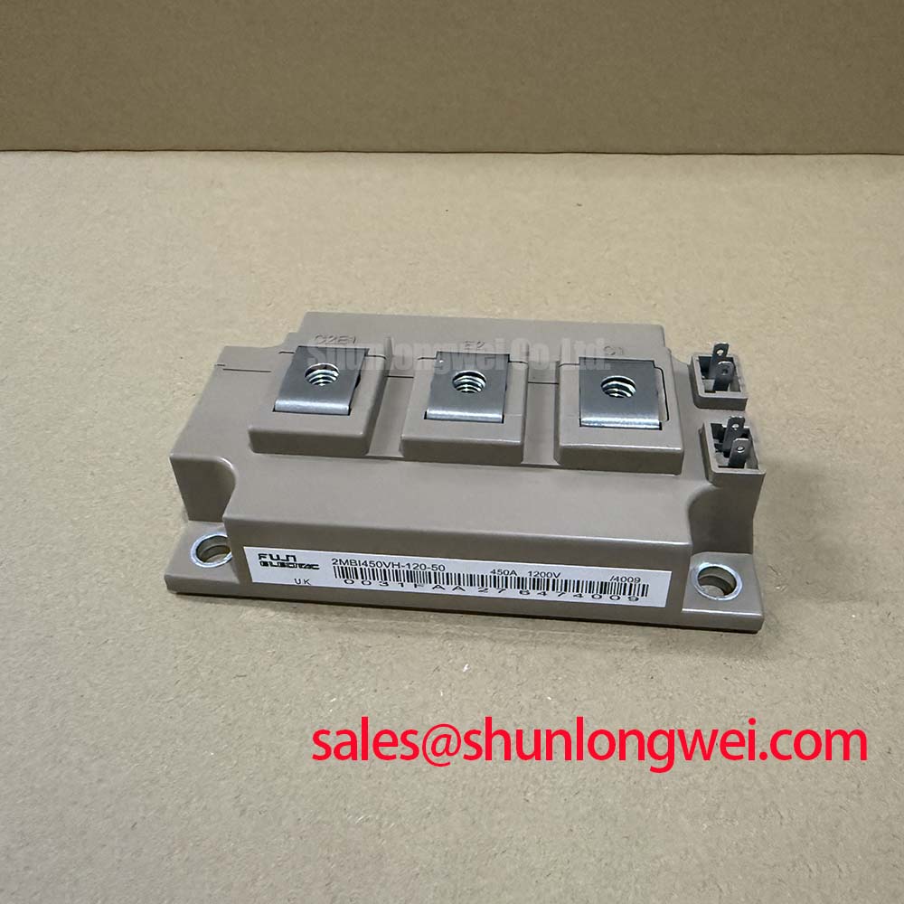
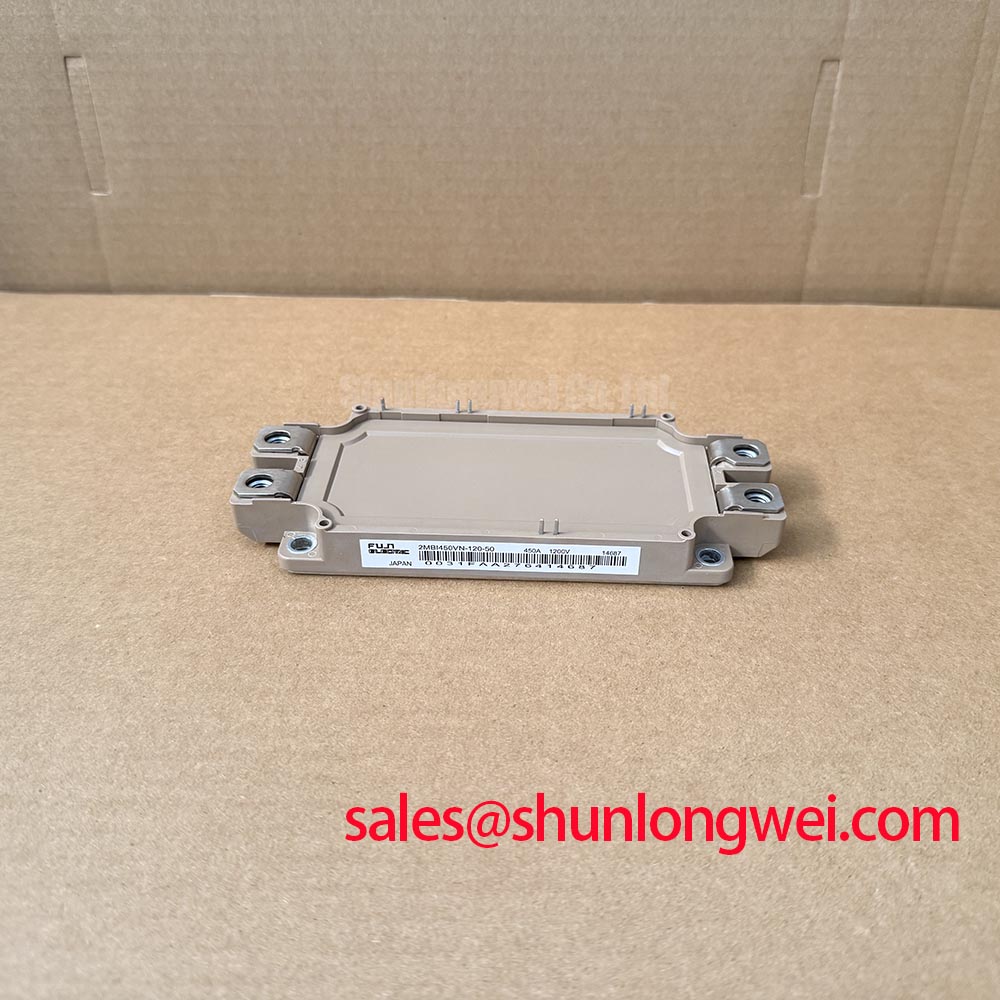
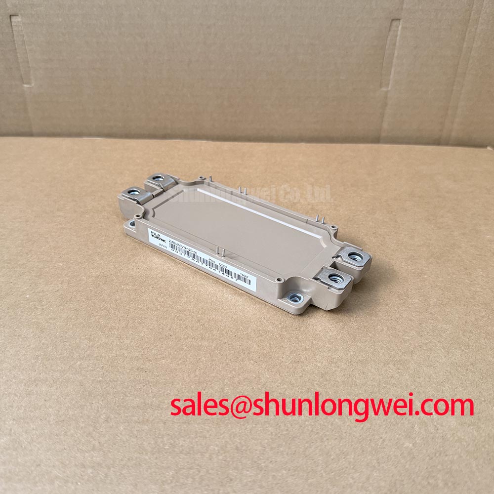
2MBI450VN-120-50 Circuit Protection & Reliability: Cosmic Ray Robustness and Voltage Derating
I check the recorded DC-link voltage and turn-off peaks before authorizing another powered test after an unexplained module failure. For the Fuji Electric 2MBI450VN-120-50, the 1200 V collector-emitter rating is an Official Specification, not a prescribed operating bus voltage. Capture the actual blocking stress during the relevant operating transitions, including regeneration, rather than relying only on the controller’s displayed bus reading.
Design Consideration: An installation’s altitude belongs in the equipment reliability assessment because terrestrial neutron exposure can affect semiconductor single-event burnout risk. An elevation threshold alone does not establish a safe operating voltage. Assessing this mechanism requires manufacturer device-specific cosmic-ray characterization, the blocking-voltage exposure profile, and installation conditions. Treat a FIT target as an equipment reliability requirement supported by applicable evidence, not as a figure calculated from the module’s voltage rating.
Keep ordinary electrical overstress separate from that assessment. Examine snubber connections, busbar joints, switching records, and protection logs for evidence of excessive blocking voltage. A damaged module or an intermittent shutdown does not identify cosmic radiation as the cause. Preserve the operating conditions and waveform records so that any specialist reliability review starts with measured evidence rather than a presumed failure mechanism.
Engineering Recommendation: Inspect terminal barriers, contamination, and the clearance between energized conductors and grounded hardware before energization. Creepage and clearance requirements depend on the equipment insulation coordination, pollution conditions, and installation environment; do not derive them from the module’s voltage class alone. Remove loose conductive debris and restore damaged barriers using the equipment service procedure.
For background on blocking stress and switching behavior, The Ultimate IGBT Knowledge Base provides supporting technical context. Use that context to organize measurements; device-specific limits and the equipment protection requirements remain the basis for acceptance.
Transient Dynamics & Electrical Design: Baseplate Contact and Mounting Screws on 2MBI450VN-120-50
Inspect the heatsink contact surface before fitting the replacement module, especially where the removed assembly left an uneven thermal-compound imprint. Check for burrs, trapped particles, damaged threads, and localized surface damage. An uneven imprint can justify further inspection, but it does not by itself prove baseplate distortion or inadequate cooling.
The supplied Official Specifications identify maximum junction-to-case thermal resistance of 0.065°C/W per IGBT, an operating junction temperature up to 150°C, and base mounting/terminal tightening torques of 3.5/4.5 N·m. The junction-to-case figure excludes the thermal interface and heatsink-to-ambient path. The junction-temperature limit is a boundary for thermal assessment, not a recommended continuous operating target.
Design Consideration: Control the thermal interface using the approved compound, application method, and mechanical drawing. The objective is continuous contact without excessive compound accumulation or trapped voids. Do not impose a generic paste thickness on this module or attempt to compensate for suspected curvature by overtightening the fasteners. Seat the module progressively in the specified mounting sequence, then complete tightening with a calibrated tool.
Field Alert: Keep the 3.5 N·m base mounting torque separate from the 4.5 N·m terminal torque; applying the terminal value to the mounting hardware can damage the assembly.
Evaluate cooling under the equipment’s actual switching frequency, load profile, ambient temperature, and airflow conditions. Higher switching frequency generally adds switching loss, while restricted cooling can raise case temperature even when load current remains unchanged. Record case-temperature measurement locations consistently and inspect filters, fans, and heatsink passages before attributing a thermal trip to the replacement module.
For transient assessment, the distinction between steady thermal resistance and time-dependent thermal impedance matters. The discussion of thermal impedance and Foster/Cauer thermal network models explains the modeling framework; it does not supply a thermal network for this particular device. Use manufacturer transient thermal data when assessing pulse loading and temperature recovery.
Assembly Integrity & Layout Architecture: Oscilloscope Waveform Verification for 2MBI450VN-120-50
Measure the gate-emitter waveform at the module connection when assessing a replacement on an existing driver board. A clean waveform at the driver output can conceal disturbance introduced by the connecting conductors. Use suitably rated differential measurement equipment and a measurement arrangement that does not introduce misleading ringing or compromise isolation.
Design Consideration: External turn-on and turn-off resistance affects switching speed, loss, and overshoot. Increasing gate resistance can reduce some switching transients while increasing switching energy; reducing it can expose parasitic inductance and coupling problems. Establish any adjustment through controlled measurements of gate voltage, collector-emitter voltage, and current, with the final values determined by the equipment design and validated operating envelope.
The supplied 1.85 V typical collector-emitter saturation voltage at Tj = 25°C is an Official Specification with a stated temperature condition. It is not a universal pass/fail reading, a cold multimeter diode-test value, or a stand-alone desaturation threshold. Evaluate conduction measurements against the applicable current and gate-drive conditions. For desaturation protection, assess detection timing and controlled turn-off together so that fault interruption does not introduce excessive voltage overshoot.
Review negative gate bias, common-mode coupling, and driver supply behavior as parts of the existing gate-drive system. Do not assign a new negative bias from a generic repair rule. When ringing appears, distinguish probe pickup from an actual gate excursion before changing components. Shorter, well-controlled gate and return paths can help reduce coupling, but their effectiveness must be checked in the assembled power stage.
During replacement sourcing, the 2MBI200VB-120-50 can be included in a documented comparison, not treated as an approved substitute. Compare current capability, terminal arrangement, mounting geometry, switching characteristics, and driver compatibility before considering any change. For a utility-scale centralized battery energy storage PCS, compatibility assessment should also cover bidirectional operating states and the converter’s protection sequence.
Where parallel modules are involved, inspect busbar symmetry and gate-path consistency. Static conduction behavior alone does not establish dynamic current sharing; compare switching waveforms and thermal behavior under representative loading before accepting the repaired assembly.
Field Diagnostics & Commissioning: Separating Driver Return from Main Current in 2MBI450VN-120-50 Topologies
Trace the driver return from the schematic to the module connector before reconnecting the gate harness. Distinguish the main emitter current path from any separately identified auxiliary emitter connection using the terminal drawing; connector position alone does not establish function. If a dedicated driver return is specified, preserve its intended routing rather than joining it arbitrarily to a convenient power connection.
Design Consideration: Shared inductance between load current and the driver reference can disturb the effective gate-emitter voltage during rapid current changes. Compare the gate waveform at the module with the driver’s local reference while observing the switching event. A disturbance that follows load-current transitions warrants examination of return routing, connection integrity, and coupling before the controller is blamed.
With the equipment isolated, the DC link discharged, and absence of voltage verified, compare cold terminal measurements between equivalent switching positions. Disconnect associated circuitry where necessary to distinguish the module from parallel paths through snubbers, drivers, or other power devices. An unusual resistance reading is a screening observation, not a complete diagnosis; record polarity, instrument mode, and connection state so the comparison remains meaningful.
Trace neighboring power stages independently. The 2MBI200S-120 is a related IGBT-module reference when reviewing associated switching circuitry, not evidence that the front end uses a particular rectifier topology. Follow the equipment schematic to identify which devices provide rectification, switching, and current commutation.
Do not substitute the 450 A continuous collector-current rating at Tc = 80°C for a diode surge-current limit or short-circuit withstand rating. Assess fault-current interruption and thermal recovery using the relevant device characteristics and protection records. Where the connected load includes a long motor cable, evaluate cable-end reflections separately from module-terminal overshoot; a corrective output filter must be selected for the complete drive and cable system.
During controlled recommissioning, observe driver supply stability, protection operation, gate behavior, and case-temperature development as loading progresses under the equipment’s approved procedure. Stop the test when a protection event or unexpected waveform appears, preserve the capture, and resolve the affected circuit before extending the operating range.