Content last revised on October 26, 2026
2MBI1400VXB-120P-54 Operational Boundaries: Evaluating Gate Drive Resistance Calibration when Replacing Legacy Modules
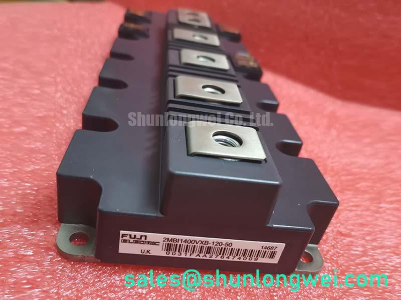
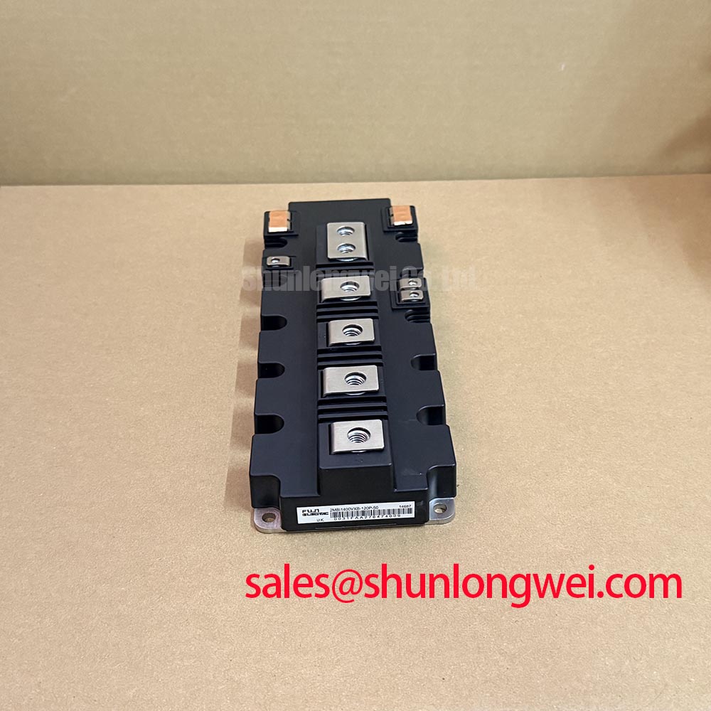
Before energizing a repaired power stage, isolate the module, inspect the gate-drive wiring, and compare the cold-state terminal condition with a known-good assembly. The 2MBI1400VXB-120P-54 is a Fuji Electric power module with a specified voltage rating of 1200.0 V and a specified current rating of 1400.0 A. The current rating depends on the manufacturer’s stated test and operating conditions. Its listed package is Fuji Power Module. These ratings identify the component boundary; actual switching stress, thermal loading, and DC-link suitability remain functions of the complete converter design.
For engineers evaluating this unit in a high-power central photovoltaic inverter, the first check is topology compatibility. A system described as a 1500 V utility-scale inverter may use internal switching nodes, isolation stages, or controlled DC-link sections with voltage conditions that differ from the installation nameplate. The system engineer should verify the actual transient voltage at the IGBT terminals, gate-drive reference, protection threshold, and cooling capability before approving a replacement.
When a modern IGBT module is installed on a legacy drive board, calibrate the external turn-on and turn-off gate resistors as a matched switching network rather than changing one resistor in isolation. The turn-on path affects current rise, diode recovery interaction, conducted noise, and switching loss. The turn-off path influences collector-emitter overshoot, ringing, and the stress seen by the clamp network. A resistor value that appears acceptable during low-voltage bench testing can behave differently when the full DC-link voltage and load current are present.
Design Consideration: begin with the legacy board’s gate-drive output impedance, isolation arrangement, gate-emitter clamp, and available peak source and sink current. Confirm that the replacement module’s gate charge and switching behavior are compatible with the driver rather than assuming that the old resistor values transfer unchanged. If turn-on ringing increases, inspect the complete gate loop, including connector pins, driver return, emitter reference, and any unused trace branches before simply increasing resistance.
Turn-off calibration should be assessed against the measured collector-emitter waveform and gate-emitter waveform at the same operating condition. Excessive resistance may slow the transition and increase switching loss, while insufficient resistance can increase ringing and electromagnetic coupling. The practical target is a controlled waveform with acceptable overshoot and thermal behavior, verified using properly rated differential voltage and current probes. Gate resistance should be selected by the system designer after switching tests, not treated as an official parameter of the module.
Legacy boards also require attention to dead-time and shoot-through protection. The two switching commands should include hardware interlock behavior, a defined fault response, and a controlled reset state. Any microsecond-scale buffer or blanking interval must be determined from the driver propagation delay, module switching behavior, load current, and converter topology. A positive temperature coefficient can assist static current sharing in operating regions where that behavior applies when multiple devices are paralleled, but dynamic sharing still depends on matched gate loops, symmetrical power paths, and simultaneous drive timing.
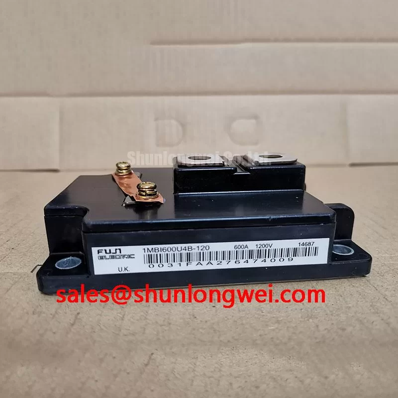
For a separate replacement evaluation, engineers may review the listed 2MBI25L-120 as a related Fuji Electric module. Package geometry, electrical ratings, gate characteristics, terminal arrangement, and thermal interface must be compared point by point before any substitution is approved.
2MBI1400VXB-120P-54 Circuit Protection & Reliability: Calibrating Baseplate Thermal Grease Layer Control
Thermal interface preparation should start with a clean, flat heatsink and a controlled application of thermal grease across the effective baseplate area. Apply only the amount recommended by the thermal-interface material and module installation procedures. The correct result is a continuous interface with minimal voiding, no exposed dry zones under the baseplate, and no excessive grease displaced into the surrounding assembly.
Baseplate curvature compensation must be treated as a mechanical contact problem. Inspect the heatsink surface for burrs, contamination, local high spots, and distortion around previous mounting locations. A thick grease layer cannot reliably correct poor flatness, while an uneven mounting surface can leave isolated hot regions even when the heatsink feels secure. Use the module manufacturer’s mechanical installation instructions for the permitted mounting sequence and torque. The torque tool should be calibrated, and the screws should be tightened progressively in a cross-pattern so that the baseplate seats evenly.
Switching frequency changes the balance between conduction loss and switching loss. At higher operating frequency, the thermal design must account for turn-on loss, turn-off loss, diode recovery interaction, gate-drive loss, and the actual cooling airflow available in the cabinet. A utility-scale inverter enclosure may experience reduced airflow because of clogged filters, fan aging, recirculation, or high ambient temperature. Thermal evaluation should therefore use measured case or heatsink temperatures and the converter’s real duty cycle rather than relying only on the nominal current rating.
The freewheel diode deserves separate attention during protection review. Its reverse-recovery softness factor, commonly identified as an S factor in device analysis, affects current commutation, voltage overshoot, and radiated EMI. The correct value must come from the applicable device data and test condition. The gate-drive network, DC-link capacitor placement, snubber, and MOV clamp should be evaluated together because a MOV selected without regard to operating voltage, energy, and clamping behavior can coordinate poorly with the semiconductor protection scheme.
⚠️ Maintenance Note: inspect heatsink airflow, thermal-interface condition, and terminal tightness during scheduled service, and investigate any rising contact temperature before returning the inverter to full load.
Where a thyristor pre-charge or protection circuit is used around the power stage, verify the gate trigger requirements using the applicable IGT and VGT characteristics. A pulse train can improve trigger reliability in some control arrangements, but pulse amplitude, duration, isolation, and fault behavior remain system-specific. Do not treat a thyristor trigger circuit as interchangeable with the IGBT gate-drive circuit.
Benchtop Waveform Tuning: Mitigating Stress via PCB Symmetry Considerations for Dual IGBT on 2MBI1400VXB-120P-54
Separate the auxiliary emitter reference used by the gate driver from the high-current emitter return path wherever the module’s terminal arrangement permits it. Shared copper can create emitter mutual coupling: the voltage developed by load current changes appears in the gate-drive reference and may alter the effective gate-emitter command. This can produce uneven switching, oscillation, or false turn-on during a fast collector-current transition.
Keep the gate loop compact, with the gate resistor positioned close to the module gate terminal and the driver return routed directly to its intended emitter reference. Avoid routing the gate trace beside the collector or high-current commutation path for long distances. The power loop should be broad and low impedance, while the control loop should remain physically separated from high di/dt copper. Clearance and creepage must follow the applicable insulation design, working voltage, pollution level, and enclosure requirements; the module listing does not establish those system-level distances.
For parallel IGBT operation, mirror the power and gate-drive geometry so that each device sees comparable stray inductance and command timing. Static current balance may benefit from positive temperature coefficient behavior in operating regions where that behavior applies, but dynamic balance is easily disturbed by unequal gate resistance, unequal emitter inductance, or different driver return paths. Compare both devices with simultaneous probes during turn-on and turn-off, looking for differences in gate plateau behavior, collector voltage slope, current sharing, and ringing frequency.
Gate turn-off bias also requires a clean reference. A negative gate bias may be considered by the system designer when high common-mode dv/dt creates false turn-on risk, but its value must be selected from the driver capability, gate-emitter limits, insulation arrangement, and switching test results. Ground bounce should be reduced through controlled return routing and suitable common-mode shielding rather than by adding an arbitrary negative voltage.
The waveform review should include the MOV and snubber response at the same time as the gate signal. If the clamp activates repeatedly during normal switching, check commutation inductance, clamp energy, device timing, and DC-link layout. The Fuji Electric reference on Fuji Electric Brake Chopper IGBT Modules provides useful manufacturer-level context for brake-chopper applications, but it does not certify a complete inverter or establish EMC compliance for the assembled equipment.
Benchtop Waveform Tuning: Mitigating Stress via Calculating Failure-in-Time Rates at High Altitude on 2MBI1400VXB-120P-54
Altitude and terrestrial neutron exposure should be addressed as a reliability assessment topic when equipment is installed above 2000 metres, especially where the DC bus operates close to the switching device’s voltage boundary. Reduced cooling performance, changed insulation conditions, and increased radiation exposure can all affect the design margin, but none can be converted into a credible FIT or Single Event Burnout rate from the module’s voltage and current ratings alone.
A defensible SEB assessment requires the actual device technology data, applied voltage distribution, altitude and location profile, neutron spectrum, operating hours, mission profile, and a recognized test or reliability model. The result should be expressed as an engineering calculation with its source conditions clearly recorded. Without that source package, use waveform surveillance and voltage-stress control as the practical field response: record peak collector-emitter voltage during representative switching events, review clamp activity, and compare the measured stress against the approved system limit.
For a 1500 V central photovoltaic inverter, the 1200.0 V rating of this module requires particular care in topology selection and transient management. The installation nameplate should not be used as a substitute for measuring the module terminals. DC-link segmentation, modulation state, commutation path, braking operation, and fault interruption can produce different voltage conditions. Engineers should verify the complete operating envelope during startup, maximum irradiance, grid disturbance, shutdown, and protection events.
Reliability records should separate electrical overstress, thermal excursions, gate-drive faults, mechanical installation issues, and environmental exposure. This makes the field investigation useful without inventing a lifetime or failure-rate claim. For topology selection and commutation behavior in appliance and power-conversion systems, the guide Resonant Topologies in Home Appliances offers additional engineering background that can support comparative circuit analysis.
When the measured waveform approaches the approved voltage boundary, reduce parasitic loop inductance, review the clamp coordination, and retune the switching transition only after confirming the gate-drive reference. The final acceptance decision belongs to the equipment design authority, based on measured electrical stress, thermal performance, protection response, and the documented application conditions.