Content last revised on September 10, 2026
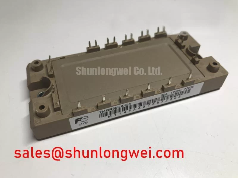
7MBR50VM120 Fuji Electric 1200V 50A PIM Power Module
Begin a replacement check by isolating the inverter, documenting the original terminal wiring, inspecting the module body and terminals for mechanical damage, and confirming the nameplate ratings before applying any test voltage. The 7MBR50VM120 is a Fuji Electric PIM power module intended for evaluation in industrial power conversion equipment, including electric material handling and forklift traction systems where its electrical, thermal, and isolation limits match the original design.
| Manufacturer | Fuji Electric |
| Product category | PIM intelligent and power module |
| Collector emitter voltage, VCES | 1200 V, Official Specification |
| Continuous collector current, IC | 50 A at Tc = 80°C, Official Specification |
| Collector emitter saturation voltage, VCE(sat) | 2.20 V typical and 2.65 V maximum at Tj = 25°C, Official Specification |
| Junction temperature, Tj | −40°C to +150°C maximum specified junction temperature, Official Specification |
| Repetitive peak reverse voltage, VRRM | 1600 V, Official Specification |
| Average output current, IO | 50 A with a 50 Hz or 60 Hz sine wave, Official Specification |
| Surge current, IFSM | 360 A for 10 ms at Tj = 150°C, Official Specification |
| Isolation voltage, Viso | 2500 V AC for 1 minute, Official Specification |
The current rating must be interpreted with the stated case temperature and the actual switching waveform. It should not be treated as a universal continuous current value under every heatsink, duty cycle, ambient temperature, or cooling condition. The Fuji Electric power semiconductor portal provides useful manufacturer-level context for assessing power module families and their documentation.
7MBR50VM120 Circuit Protection and Reliability: Negative Gate Bias and Active Miller Clamp
During field replacement, inspect the gate driver board as carefully as the power module. A module that measures normally at room temperature can still be exposed to excessive gate transients if the driver supply, isolation barrier, gate resistor network, or emitter return path has been damaged. Confirm that the replacement follows the original terminal assignment and that the driver logic is compatible with the system documentation.
High common-mode voltage movement can couple through the module’s internal capacitances and raise the off-state gate potential. A negative gate bias can be evaluated as a Design Consideration when the original driver architecture supports it, but the suitable value is system-determined by gate-emitter limits, driver isolation, switching speed, and protection behavior. An active Miller clamp is another system-level option for holding the inactive gate low during a rapid collector voltage transition. The module itself should not be described as containing a particular clamp function unless the applicable Fuji Electric documentation confirms it.
For a forklift traction inverter, inspect the driver isolation barrier for common-mode transient immunity appropriate to the switching environment. Check gate-to-emitter behavior with the DC bus discharged, compare each phase against a known-good channel, and use an oscilloscope with suitable differential and isolated measurement methods before reconnecting the motor. Unusual gate ringing, unequal turn-on delay, or a gate waveform that changes with phase current may indicate a driver, layout, or parasitic coupling issue rather than a module-only fault.
High-voltage clearance and creepage must be reviewed across the complete assembly. Keep conductive contamination, loose hardware, cable shields, and mounting brackets away from the high-potential terminals. The required spacing is determined by working voltage, pollution environment, insulation system, and the applicable equipment standard. The stated 2500 V AC isolation voltage for one minute is an official module specification, not an automatic certification of the finished inverter.
Field Alert: Disconnect the DC bus and verify stored energy has fallen to a safe level before unplugging the gate-drive connector or handling the module terminals.
Preventing Spurious Faults: DC Bus and Low-Inductance Connection Design
When a failed module is replaced, examine the DC bus structure for discoloration, loose laminated conductors, cracked capacitors, and damaged suppression components. The switching loop should be kept compact so that stray inductance does not convert current change into an excessive voltage spike. In practical terms, the transient peak rises with DC bus voltage, loop inductance, and switching current slew rate; the acceptable peak must be verified on the actual inverter with a properly rated probe.
A laminated busbar or closely coupled planar conductor arrangement can reduce loop area when its geometry is compatible with the module terminals and insulation requirements. This is an Engineering Recommendation, not a guaranteed construction requirement for this model. The system designer should validate the arrangement during double-pulse or controlled switching tests, checking the collector-emitter peak against the module’s voltage rating and the selected operating margin.
Line-frequency ripple from the rectifier and battery or DC-link transients can also affect the module. In a traction system, inspect the DC-link capacitor bank, precharge circuit, contactors, braking path, and cable connections before attributing a fault to the IGBT module. The related 7MBR50SA120-50 may be assessed as a neutral reference for an associated rectifier stage, but electrical compatibility must be verified from the complete system schematic.
RC snubbers, MOVs, active clamps, and fast semiconductor fuses should be evaluated as a coordinated protection network. An MOV selected without regard to repetitive DC voltage, energy, and fault behavior may introduce leakage or fail during a sustained overvoltage event. Likewise, fuse selection requires comparison of the semiconductor short-circuit withstand behavior with the fuse’s clearing characteristics and I²t specification. These are system protection decisions; the published module ratings do not define a complete fuse or snubber prescription.
Benchtop Waveform Tuning and High-Altitude Reliability Assessment
Use a controlled low-energy test first. Confirm gate timing, dead time, phase-current symmetry, diode commutation, and DC-link behavior before applying the full operating bus. The official 1200 V VCES rating establishes the collector-emitter voltage boundary, while the 1600 V VRRM, 360 A IFSM, and temperature ratings describe separate conditions that should not be combined as one universal operating limit.
Reverse-recovery behavior in the freewheel path can increase voltage overshoot, ringing, and radiated interference. Observe the diode current transition and the collector-emitter waveform together rather than diagnosing EMI from a single probe trace. The reverse-recovery softness factor is device and operating-condition dependent, so the engineer should compare measured behavior with the original module documentation and the complete commutation network.
Altitude, terrestrial neutron exposure, and single-event burnout are high-risk reliability subjects requiring authoritative device data and application-specific testing. No FIT rate, SEB probability, operating-life figure, or altitude derating value should be assigned to this module without a qualified source such as a manufacturer reliability document, applicable JEDEC material, or an authorized test report. At elevated installation sites, designers should review insulation coordination, cooling performance, switching stress, and DC-bus headroom as separate factors, then validate the finished equipment under representative conditions.
For broader technology context, the Wide Bandgap Revolution article can support comparative system discussions, but it should not be used to infer unlisted electrical or reliability characteristics for this silicon power module.
Transient Dynamics and Gate-Drive Loop Geometry
Keep the gate-drive signal path physically separate from the high-current commutation path. The auxiliary emitter return used by the driver should be routed according to the module’s documented terminal arrangement and should not share a long, high-current copper path with the power emitter connection. Shared impedance can create emitter voltage movement at the driver reference, producing apparent gate oscillation or unequal switching between phases.
When checking a suspected oscillation, measure gate-to-emitter voltage directly at the module terminals and compare it with the driver output at the isolation barrier. Also inspect gate resistor solder joints, driver supply decoupling, isolation components, and any damaged clamp or protection network. A waveform that looks acceptable at the driver but unstable at the module points toward layout or return-path coupling; a distorted waveform at both points requires investigation of the driver supply and control timing.
Mechanical installation affects thermal and electrical reliability. Clean the mounting surfaces, use a uniform thermal interface layer appropriate to the assembly, and tighten the hardware according to the fastener and heatsink specification supplied for the equipment. Designers should verify thermal impedance, case temperature, contact flatness, and pressure distribution after installation rather than relying only on a visual inspection. A replacement is suitable only after its terminal configuration, protection network, gate-drive behavior, cooling arrangement, and measured switching margins have been checked against the original system.