Content last revised on October 24, 2026
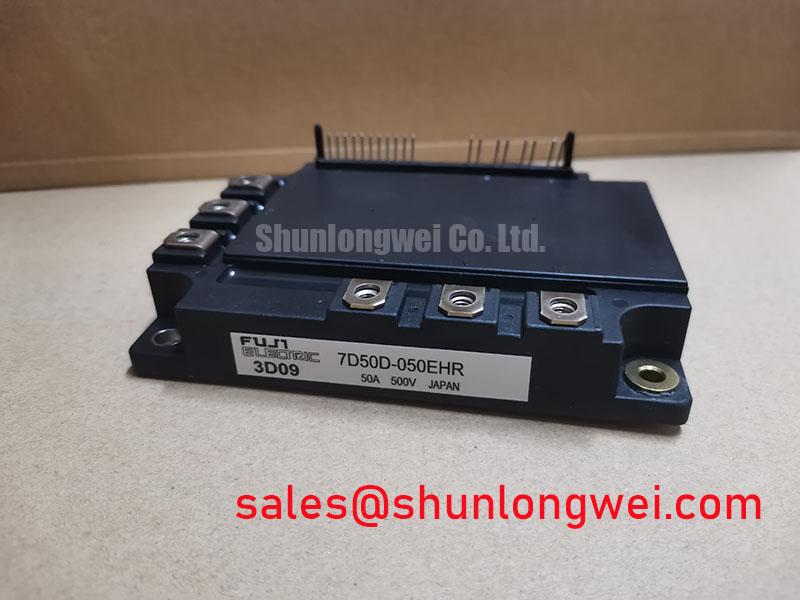
7MBR50SA-060 Specifications and Application Overview
When a compact inverter reports an intermittent overcurrent trip, isolate the DC link, confirm the gate-driver supply is discharged, and inspect the switching path before removing the power module. The Fuji Electric 7MBR50SA-060 is specified for a 600 V collector-emitter voltage and a 50 A continuous collector current at Tc = 25°C. Its listed collector power dissipation is 200 W for one device, while the repetitive peak reverse voltage is 800 V and the average output current is 50 A.
For the stated test condition of IC = 50 A and VGE = 15 V, the collector-emitter saturation voltage is 1.9 V typical and 2.4 V maximum. These are Official Specification values and should be kept separate from system-level limits determined by switching frequency, thermal impedance, DC-link behavior, motor-cable length, and the actual gate-driver circuit. The device may be evaluated in compact industrial inverters and high-speed CNC spindle drives, subject to complete electrical, thermal, mechanical, and protection verification.
The manufacturer context can be reviewed through the Fuji Electric Power Semiconductors Portal. In a repair workflow, compare the installed module’s terminal arrangement, gate-drive reference, mounting interface, and protection network with the equipment documentation before energizing the replacement.
| Official Specification | Value | Condition |
|---|---|---|
| Collector-emitter voltage, VCES | 600 V | Specified rating |
| Continuous collector current, IC | 50 A | Tc = 25°C |
| Collector-emitter saturation voltage, VCE(sat) | 1.9 V typical, 2.4 V maximum | IC = 50 A, VGE = 15 V |
| Collector power dissipation, PC | 200 W | One device |
| Repetitive peak reverse voltage, VRRM | 800 V | Specified rating |
| Average output current, IO | 50 A | Specified rating |
7MBR50SA-060 Circuit Protection and Reliability: Preventing Spurious Power-Up Shoot-Through
Power-up shoot-through is best addressed by controlling the order in which the auxiliary driver supply, gate signals, and high-voltage DC link become active. The gate driver should reach its valid operating state before the DC link is applied, and the control logic should hold both switching commands inactive until the driver’s undervoltage lockout status is stable. This is a Design Consideration for the complete converter, not an additional Fuji Electric rating for the module.
A negative turn-off bias may be evaluated where the switching environment has substantial common-mode displacement or rapid collector-voltage transition. The requested evaluation range of −5 V to −15 V should be treated as an Engineering Recommendation for driver design review only; the final gate voltage, absolute maximum limits, turn-on threshold behavior, and driver compatibility must be established from the applicable gate-drive documentation and bench testing. The negative rail must not be allowed to introduce excessive gate-emitter stress during startup, shutdown, or an isolated-driver fault.
During commissioning, monitor the driver auxiliary rails independently from the DC-link voltage. A clean logic enable signal does not prove that the isolated gate supply is ready. Check the UVLO output or fault feedback, confirm that the gate output remains inactive during undervoltage conditions, and verify that the control board cannot release PWM when the high-side and low-side driver channels have different startup delays. A failed bootstrap supply, floating driver reference, or incorrectly sequenced enable line can produce a switching event before the protection logic has authority.
The power loop should use a compact, symmetrical connection between the DC-link capacitors, the module terminals, and the switching return path. Minimize parasitic loop inductance to reduce turn-off overshoot, then verify the measured peak voltage against the module’s 600 V VCES rating under the intended switching condition. The busbar arrangement, capacitor placement, gate-return routing, and snubber location are system-dependent; they should be validated with a properly rated differential probe and a current probe rather than inferred from a low-voltage continuity test.
For field replacement, record the original gate polarity and driver reference before disconnecting the module. A control connector that appears mechanically compatible can still have a different signal reference or protection arrangement. Where the repair requires a related device for comparison, the 7MBR15SA060D-01 can be reviewed as a separate Fuji Electric module, but electrical interchangeability must be established by the system engineer rather than assumed from family naming.
⚡ Safety Interlock Note: Keep the high-voltage DC link inhibited until the auxiliary driver supply, UVLO interlock, and gate-off state have been observed during repeated cold-start tests.
Benchtop Waveform Tuning: Mitigating Stress from Cres-Induced Gate-Voltage Spikes on 7MBR50SA-060
High dv/dt can couple displacement current through the effective collector-gate capacitance and lift a supposedly inactive gate above its intended off-state. This Cres-related gate disturbance is influenced by the gate-loop impedance, common-emitter or power-return inductance, driver sink capability, and the physical spacing between the switching path and control wiring. Treat the result as a waveform problem: observe the gate-emitter voltage at the module terminals while simultaneously observing collector-emitter voltage and phase current.
A dedicated low-impedance active Miller clamp is a Design Consideration when the driver must hold the inactive gate firmly during the opposing device’s voltage transition. The clamp should be connected with a short, controlled return path and should not share a long inductive segment with the high-current emitter or power return. A negative turn-off supply in the −5 V to −15 V evaluation range may be considered for suppressing unwanted gate elevation, but the selected value remains a system decision governed by the driver, isolation barrier, gate-emitter rating, and switching waveform.
Before connecting the driver, identify the module’s collector, emitter, gate, and auxiliary terminals from the applicable terminal drawing. Do not use a connector’s physical keying as proof of electrical compatibility. Confirm the gate-return reference with the original harness documentation, then check for unintended continuity between the control return and the high-current power path. When the measured gate waveform differs between the upper and lower switching positions, investigate layout asymmetry, probe placement, driver propagation delay, and local return inductance before changing the gate resistor.
Bench testing should begin at a controlled DC-link level and with a current-limited supply. Increase switching stress only after confirming that the inactive gate remains within the intended off-state throughout the opposing device’s voltage transition. A waveform that looks acceptable at the driver output may be substantially different at the module pins because of connector inductance and shared return paths. Use a short spring connection or an appropriate differential measurement method at the gate-emitter terminals, and keep the probe loop away from the commutation path.
Mechanical stability also affects waveform repeatability. Busbar joints, laminated conductors, terminal hardware, and cable supports should resist movement under motor-drive vibration and electromagnetic force. A changing contact surface can appear as intermittent gate noise or current imbalance even when the control firmware is unchanged. Mounting torque is a Design Consideration that must follow the module’s mechanical documentation and the selected hardware; it should not be substituted with a generic value.
For the surrounding topology, the 7MBR50SD120 may be reviewed as a related rectifier or front-end device in a converter architecture. Its presence does not establish a complete protection solution for the 7MBR50SA-060. The DC-link capacitor arrangement, rectifier commutation, braking path, and motor-side switching network each contribute different transient conditions and require separate measurements.
The Fuji Electric portal provides a useful manufacturer-level reference point for power semiconductor product families. By contrast, IO-Link is an industrial sensor and actuator communication protocol, not a substitute for an isolated gate-drive interface or a power-module protection signal. Keeping these functions separate prevents a control-network assumption from being applied to the high-energy switching path.
Preventing Spurious Faults: Long Motor Lead Reflected Wave Voltage Guidelines for 7MBR50SA-060
Long motor leads behave as a transmission path rather than an ideal wire, so the inverter output edge can reach the motor with a different voltage and current relationship from the one measured at the module terminals. An impedance mismatch at the motor, cable termination, or inverter output can create reflected waves that return toward the switching bridge. Under unfavorable conditions, the terminal transient can approach approximately twice the incident step voltage, making the motor-side waveform and the module-side waveform essential parts of the same diagnosis.
The 600 V VCES rating of the 7MBR50SA-060 is an Official Specification limit, not a target for repeated transient operation. When a long cable is used, the system engineer should examine the peak collector-emitter voltage at the module, the phase-to-phase motor voltage, and the common-mode voltage relative to protective earth. Compare these traces at the actual cable length and motor load. A short bench cable can conceal a reflected-wave problem that appears only after the production harness is installed.
Output filters, dv/dt filters, and motor chokes are Design Considerations when the cable impedance and switching edge produce unacceptable terminal stress, bearing-current concerns, or motor insulation stress. Their selection depends on the inverter carrier strategy, motor impedance, cable construction, filter resonance, thermal behavior, and protection coordination. Do not select a filter from the 50 A module rating alone. Verify the filter’s effect on switching loss, current regulation, fault detection, and the voltage observed directly at the module terminals.
When troubleshooting an overcurrent or ground-fault alarm, first compare the inverter output waveform with a known-good cable arrangement, then repeat the observation with the installed motor and cable. Look for ringing that changes with cable routing, motor connection, or filter insertion. A waveform change after moving the cable away from the DC bus can indicate magnetic coupling or an altered return path, while a change after adding a termination network may indicate transmission-line interaction. These observations narrow the fault without assigning a single cause prematurely.
Keep the DC bus, phase conductors, and protective-earth conductors arranged so that high-current loops remain compact and control wiring is not routed alongside the most aggressive switching nodes. Cable shields and motor-frame connections should follow the equipment’s EMC and safety architecture. The module itself cannot independently claim compliance with complete equipment standards such as CISPR or EN 55011; compliance depends on the assembled inverter, enclosure, wiring, filter network, grounding, and operating conditions.
MOVs, RC snubbers, active clamps, and other overvoltage networks can be coordinated with the bridge and output filter as part of a system protection study. The MOV clamping characteristic, energy capability, leakage, aging behavior, and placement must be evaluated against the actual transient waveform. Place protective components so their current path does not add unnecessary inductance, and confirm that a protection device failure cannot leave the gate driver exposed to an uncontrolled switching state.
For installations involving solar or energy-storage inverter topologies, the Peak Efficiency in Solar and Energy Storage reference can support broader topology and test planning. It should be used as an application reference rather than as a substitute for the 7MBR50SA-060 electrical specification or the original equipment manufacturer’s protection design.
Parallel-device operation also requires measured current sharing rather than an assumption based on positive temperature behavior. Static sharing is affected by saturation-voltage spread, gate-drive matching, thermal coupling, and layout resistance; dynamic sharing is affected by propagation delay, stray inductance, and switching-speed mismatch. If multiple devices are used in a system, designers should verify current balance during startup, steady operation, overload response, and turn-off transients while checking that the combined protection network reacts consistently across each current path.