Content last revised on June 12, 2026
Fuji Electric 6MBI100U2B-060 IGBT Module: Enhancing Efficiency in Industrial Inverters
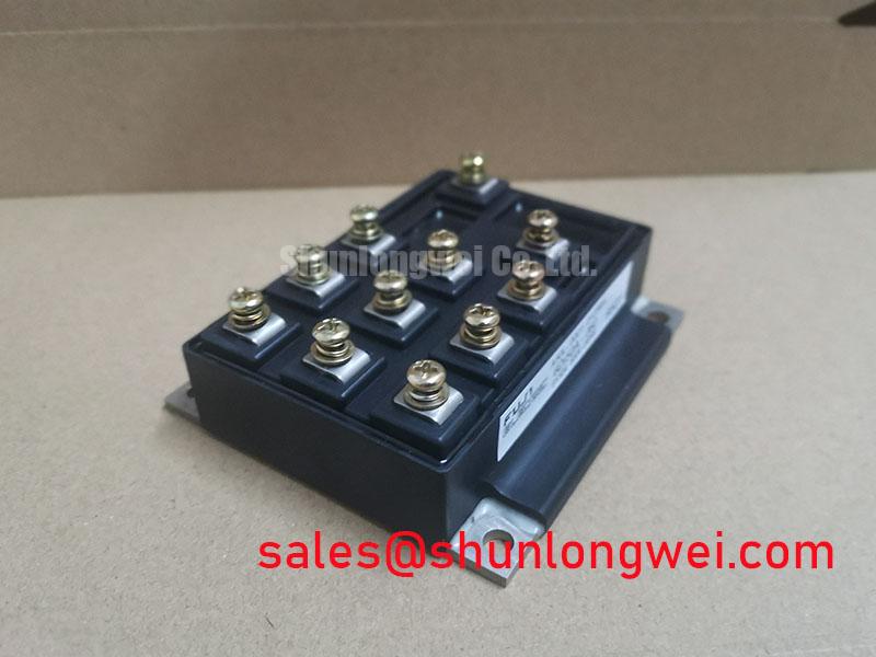
The 6MBI100U2B-060 is a high-performance IGBT Module designed by Fuji Electric, featuring a 6-pack configuration that integrates six insulated gate bipolar transistors with flyback diodes into a single, compact housing. Engineered for 600V and 100A operation, this module belongs to the renowned U-series, which is specifically optimized for low-loss switching and high-reliability industrial applications. For engineers prioritizing power density and thermal margin, the 6MBI100U2B-060 serves as a critical building block in developing efficient motor control systems and power converters.
Key Benefits: High-speed switching capability and simplified thermal management due to low VCE(sat). What is the primary advantage of the 6MBI100U2B-060 saturation voltage? Low saturation voltage minimizes conduction losses, significantly improving overall energy efficiency in continuous-load operations. For compact motor controllers requiring high power density and reliable thermal management, this module is the optimal choice.
Key Parameter Overview
Decoding the Specs for Enhanced Thermal Reliability
Understanding the electrical boundaries of the 6MBI100U2B-060 is essential for robust system design. The following technical specifications highlight the module's capacity for high-power handling within the U2B package architecture.
| Feature Category | Technical Parameter | Specified Value |
|---|---|---|
| Maximum Ratings | Collector-Emitter Voltage (Vces) | 600V |
| Current Capacity | Continuous Collector Current (Ic) | 100A (at Tc=80°C) |
| Switching Performance | Saturation Voltage (Vce(sat)) | 1.70V (Typical) |
| Isolation Voltage | Viso (AC 1 min) | 2500V |
| Thermal Management | Junction Temperature (Tj) | Up to +150°C |
Download the 6MBI100U2B-060 datasheet for detailed specifications and performance curves.
Application Scenarios & Value
Achieving System-Level Benefits in High-Frequency Power Conversion
In the realm of industrial automation, engineers often face the challenge of managing heat in confined enclosures. The 6MBI100U2B-060 addresses this by offering a low-profile 6-pack structure that reduces parasitic inductance compared to discrete alternatives. This is particularly beneficial for a Variable Frequency Drive (VFD) or a Servo Drive, where rapid switching frequencies are required to maintain precise motor control without incurring excessive electromagnetic interference (EMI).
Consider a scenario involving high-density industrial robotics. The module’s integrated 6-pack design allows for a significantly smaller PCB footprint, enabling more compact Servo Drive units. When compared to larger modules like the 6MBI450U-120, which is suited for heavy-duty 1200V systems, the 6MBI100U2B-060 provides a specialized solution for 200V-400V class systems where efficiency and space are the primary design drivers. This level of integration supports the broader industry shift toward industrial 4.0 standards, where energy conservation and equipment miniaturization are paramount.
Furthermore, the 6MBI100U2B-060 is frequently utilized in UPS (Uninterruptible Power Supply) systems. Its robust Short-Circuit Withstand Time ensures that the power stage remains intact during transient faults, protecting sensitive downstream equipment. By leveraging the U-series technology, designers can achieve a lower total cost of ownership through reduced heatsink requirements and increased hardware longevity. For further insights into selection, see our guide on IGBT selection beyond Vce(sat).
Technical & Design Deep Dive
Thermal Management and Structural Integrity in the U-Series
The internal architecture of the 6MBI100U2B-060 utilizes a DBC (Direct Bonded Copper) substrate, which acts as the thermal highway of the module. To visualize this, think of the thermal resistance (Rth) as a bottleneck in a plumbing system; the Fuji Electric design minimizes this bottleneck, allowing heat to flow seamlessly from the silicon junction to the baseplate. This efficiency is critical when operating near the 150°C junction temperature limit, as it prevents thermal runaway and ensures stable Switching Loss characteristics over time.
Designing for long-term reliability also requires careful Gate Drive consideration. The 6MBI100U2B-060 exhibits low gate charge, which reduces the power requirements for the gate driver IC. However, to prevent unintended turn-on due to the Miller effect, designers should implement a negative gate bias or an active Miller Clamp. This is especially important in high-performance inverter topologies where high dV/dt transitions are common. For a comparison of integrated solutions versus discrete builds, reference our analysis on IPM vs. Discrete IGBT frameworks. Integrating this module effectively requires balancing switching speed with overshoot voltage, typically managed through optimized Snubber Circuit placement and DC-link busbar design.
Frequently Asked Questions
How does the low Vce(sat) of the 6MBI100U2B-060 impact heatsink sizing in a 100A application?
The low Vce(sat) of typically 1.70V directly reduces conduction losses. Since power dissipation (P = Vce(sat) * Ic) is lower, the requirement for thermal dissipation is reduced, allowing for smaller heatsinks or higher current density within the same thermal footprint.
What are the critical gate drive requirements to ensure the 6MBI100U2B-060 stays within its Safe Operating Area (SOA)?
To maintain operation within the Safe Operating Area, the Gate Drive must provide a stable voltage (typically +15V) with sufficient peak current for fast charging of the input capacitance. Furthermore, the Short-Circuit Withstand Time of 10 microseconds must be matched with a gate driver that features desaturation protection to prevent module failure during a fault.
For engineering teams evaluating power components for upcoming projects, the Fuji Electric 6MBI100U2B-060 represents a mature, high-performance solution for mid-range power conversion. For deeper technical exploration of IGBT Module architecture and its role in modern power electronics, please visit the Fuji Electric official semiconductor portal or review our comprehensive IGBT engineering guide.