


Content last revised on September 24, 2026
6DI50C-050 Thermal-Electrical Optimization for Regenerative DC-Bus Surge Control
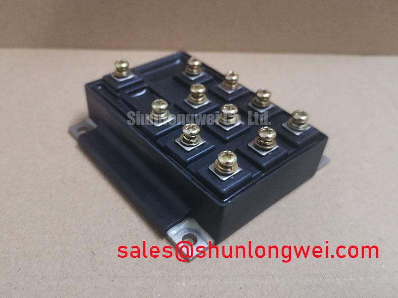
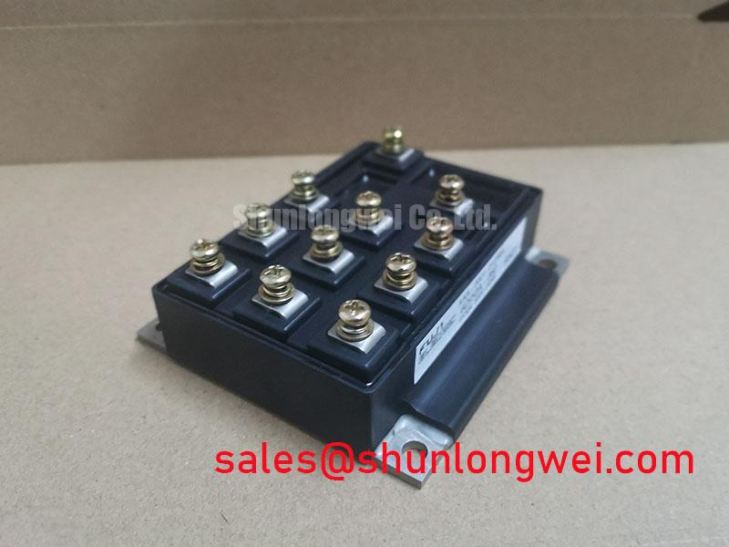
Before connecting the replacement, inspect the package, confirm the nameplate rating, and compare the cold-state terminal readings with a known-good assembly. The 6DI50C-050 is a Fuji Electric Power Transistor Module with an official voltage rating of 600 V and an official current rating of 50 A. These are device ratings; the allowable operating point in an inverter welder or medium-frequency induction heating supply remains dependent on switching frequency, cooling, duty cycle, bus conditions, and the original equipment design.
| Manufacturer | Fuji Electric |
| Part number | 6DI50C-050 |
| Product category | Power Transistor Module |
| Rated voltage | 600 V, Official Specification |
| Rated current | 50 A, Official Specification |
When evaluating a repair, verify the original schematic, gate-drive arrangement, cooling method, protection circuit, and terminal assignment before applying power. Fuji Electric’s power semiconductor and IPM module reference and its power semiconductor portal provide useful manufacturer-level context, but the equipment designer must confirm the exact circuit interface for this part.
In a regenerative drive or welding power supply, a braking transistor can route deceleration energy into a resistor when the DC bus rises. For the 6DI50C-050, the practical engineering task is to verify that the switching device, resistor, pulse duration, cooling path, and bus-voltage limit are compatible as one system. The resistor must absorb the actual kinetic or stored energy without exceeding its short-duration and average thermal limits. The module’s 600 V rating should be treated as an official device boundary, not as permission to operate the DC bus close to that value without measured switching margin.
Keep the braking-current loop compact and physically separated from sensitive gate-drive and feedback wiring. Designers should verify turn-off overshoot with an oscilloscope using an appropriate differential probe, then compare the measured peak with the equipment’s validated voltage margin. If a braking event produces unexpected bus rise, inspect the resistor, contactors, current sensor, gate signal, and DC-link capacitor condition rather than assigning the symptom to the transistor alone. Semiconductor fuse coordination also requires checking the fuse clearing characteristic and the module’s documented short-circuit or energy limits; an I²t comparison is an engineering calculation only when the relevant manufacturer data is available.
For cross-reference work, engineers may also review the neutral product information for QM200HA-HK, while confirming voltage, current, package, pinout, and switching characteristics independently before considering any circuit substitution.
6DI50C-050 Gate-Control Optimization and Miller-Current Suppression
High dv/dt at the switching node can couple through internal capacitances and disturb the opposite gate. A suitable gate driver should provide a low-impedance turn-off path, controlled propagation delay, and adequate common-mode transient immunity for the actual switching environment. An active Miller clamp can be evaluated when the driver architecture supports it, but its threshold, timing, current capability, and isolation behavior must be verified from the driver documentation and bench measurements. A negative gate bias is a system design choice, not an official 6DI50C-050 parameter supplied in the stated data.
For parallel modules, symmetrical busbar geometry and matched gate-drive paths help reduce unequal stray inductance. The positive temperature coefficient associated with many IGBT conduction characteristics can support static current sharing, but it does not remove dynamic imbalance caused by unequal wiring, gate timing, thermal gradients, or emitter coupling. Check each branch during turn-on and turn-off with isolated probes. Industrial inverter welders may also use optocouplers or digital isolators; their CMTI performance should be checked against measured common-mode transients rather than assumed from the isolation rating alone.
6DI50C-050 Reliability Assessment for High-Altitude Switching Systems
There is no supplied field dataset or authoritative FIT, SEB, cosmic-ray, or altitude-derating value for this specific part in the stated product information. A responsible reliability assessment therefore requires measured bus voltage, switching waveform, junction-temperature estimation, cooling conditions, and the applicable manufacturer reliability documentation. Terrestrial radiation exposure and altitude-related cooling changes may be considered during system qualification, but a numerical failure rate must not be inferred from the 600 V rating.
For installations above the original equipment’s qualified environment, designers should review DC-bus headroom, creepage, clearance, enclosure condensation control, and thermal resistance as separate engineering topics. During troubleshooting, record the operating state preceding failure, inspect semiconductor fuses and gate-drive supply behavior, and compare the damaged switching position with the companion positions. The technical discussion in Resonant Topologies in Home Appliances can help engineers relate switching topology to stress distribution without treating topology guidance as a device-specific guarantee.
Assembly Integrity and Layout Architecture for Dual-IGBT Circuits
During installation, keep the high-current emitter return separate from the auxiliary gate-reference return wherever the equipment layout provides those distinct paths. Shared copper can create emitter mutual coupling, causing apparent gate-voltage movement, ringing, or unequal switching between parallel devices. The correct arrangement depends on the actual terminal definition and the original board layout, so confirm continuity and routing against the equipment drawing before modification.
Minimize the commutation loop area, maintain consistent busbar geometry, and route gate-drive conductors away from high-current switching nodes. Insulation spacing must be checked against the working voltage, pollution environment, material group, and applicable equipment standard; no universal clearance value should be assigned to this module without those conditions. After assembly, inspect solder joints or bolted interfaces, verify thermal contact, and test the gate waveform at operating temperature.
Maintenance Note: De-energize and discharge the DC link before touching the module, and periodically inspect heatsink airflow, thermal-interface condition, terminal tightness, and contact-temperature trends.